
|

|
Dual Active Bridge Development Board (Part-No. ) |

|
|||
|
Content
|
||||||
|
|
|
Dual Active Bridge Development Board (Part-No. ) |
|
|||
|
Content
|
||||||
The firmware overview indicates that the power controller state machine and fault handler are executed every 100 microseconds by the scheduler. Additionally, the GUI handler operates every 10 milliseconds, while the LED and fan operations, along with temperature checks, are performed every 100 milliseconds.
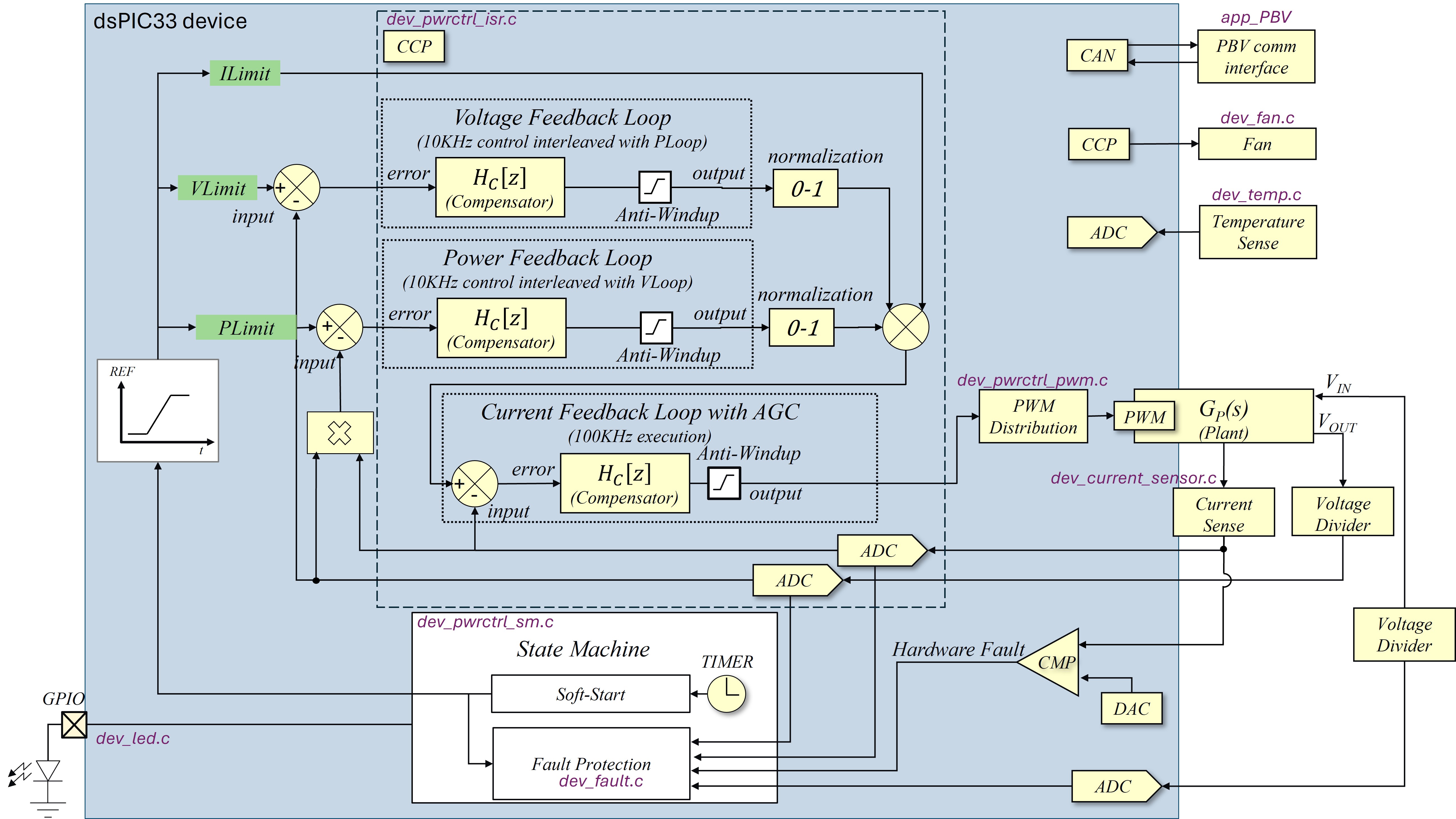
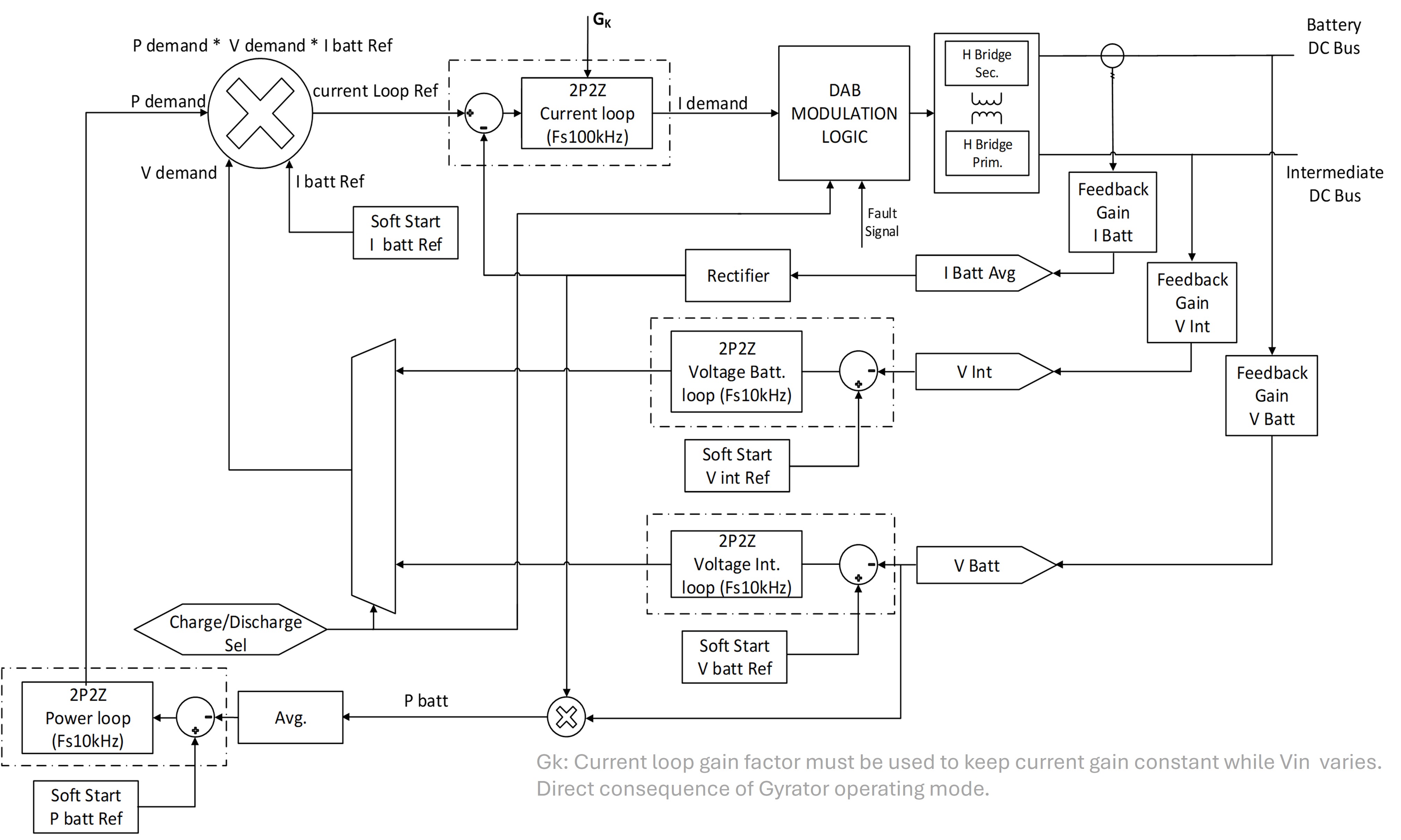
The system has a single interrupt source, the ControlLoop_Interrupt_CallBack(), which is executed every 10 microseconds. This callback measures voltages and currents on the DAB board using an ADC and feeds the data to three control loops. The Voltage and Power loops operate at 10 kHz, interleaved, while the Current Loop operates at 100 kHz.
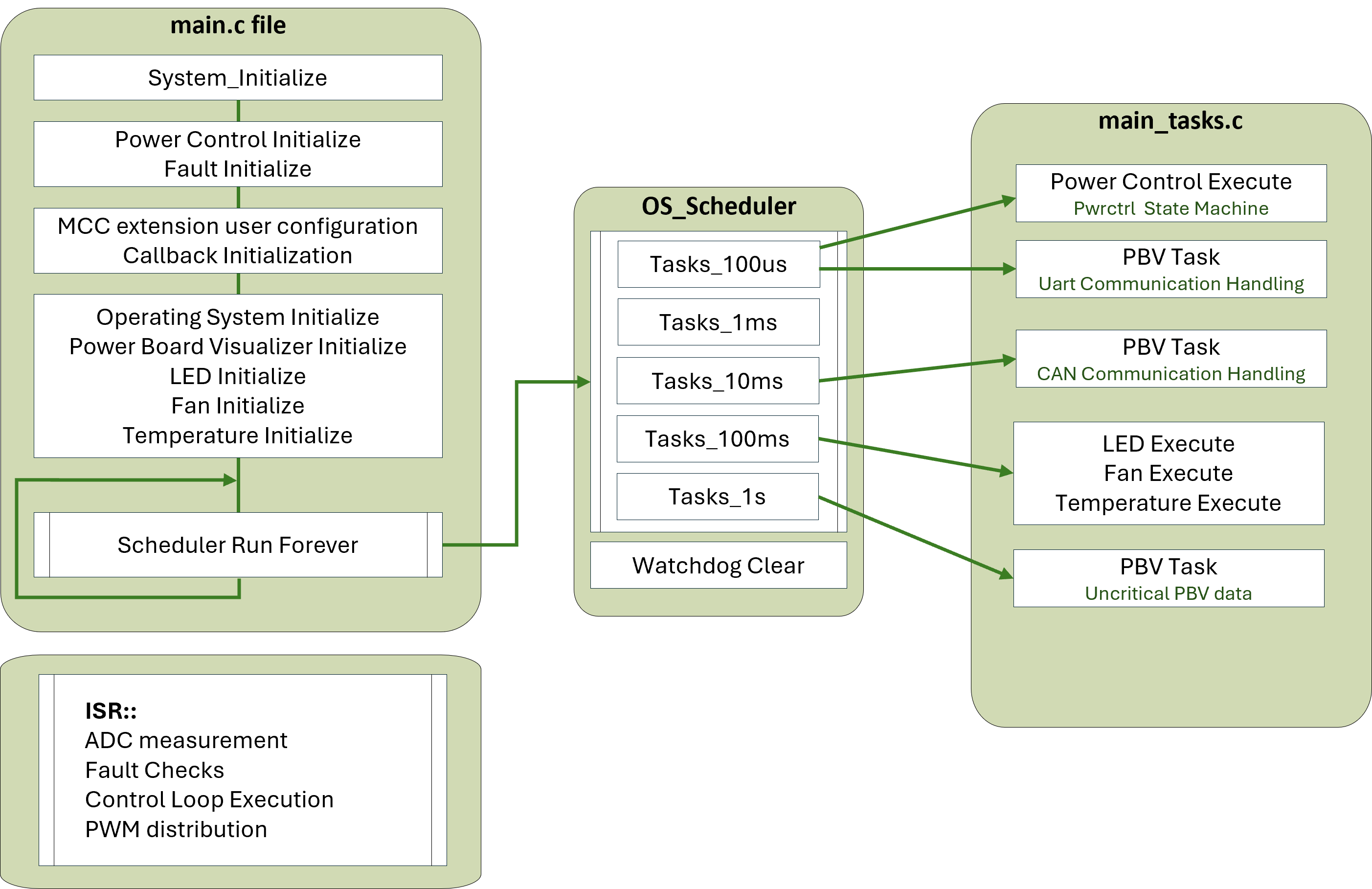
The Microchip Code Configurator (MCC) is utilized to set up peripherals. This configuration occurs at run-time at the beginning of the main() function, prior to the initiation of the background loop.
The project files are organized as follows:
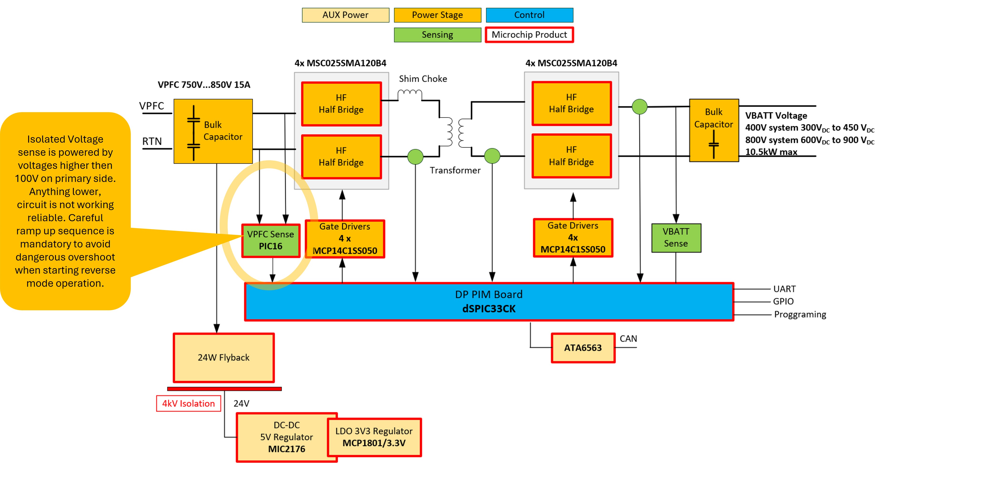
The firmware block diagram illustrates the use of the dspic33C for a Dual Active Bridge converter. The following provides a detailed explanation of the firmware development for this application.
The DAB board operates in two levels, capable of outputting either 400V or 800V, depending on the user-specified settings. These voltage levels are controlled by two defines in the config/config.h file:
#define DCDC400V_SYSTEM
The 400V battery system operates within a voltage range of approximately 300V (discharged) to 450V (fully charged).
#define DCDC800V_SYSTEM
The 800V battery system operates within a voltage range of approximately 600V (discharged) to 900V (fully charged).
Typically, a single-phase totem pole combined with a DAB DC/DC converter is used for the 400V system (450V input, 300V to 450V output). For the 800V system, a three-phase totem pole combined with a DAB DC/DC converter is recommended (800V input, 600V to 900V output).
When switching between modes, the fault protection thresholds are automatically adjusted to match the selected voltage range.
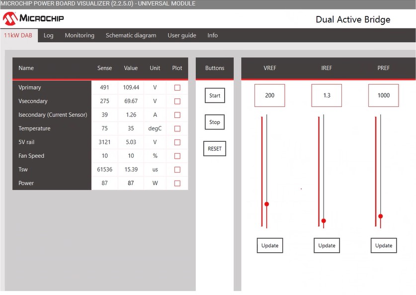
The Dual Active Bridge (DAB) application is designed to operate in two distinct modes: forward and reverse. This dual-mode capability allows the system to function bidirectionally, transferring power in both directions. Users can easily switch between these operational modes using the Power Board Visualizer, a tool that provides a graphical interface for managing and configuring the power board settings.
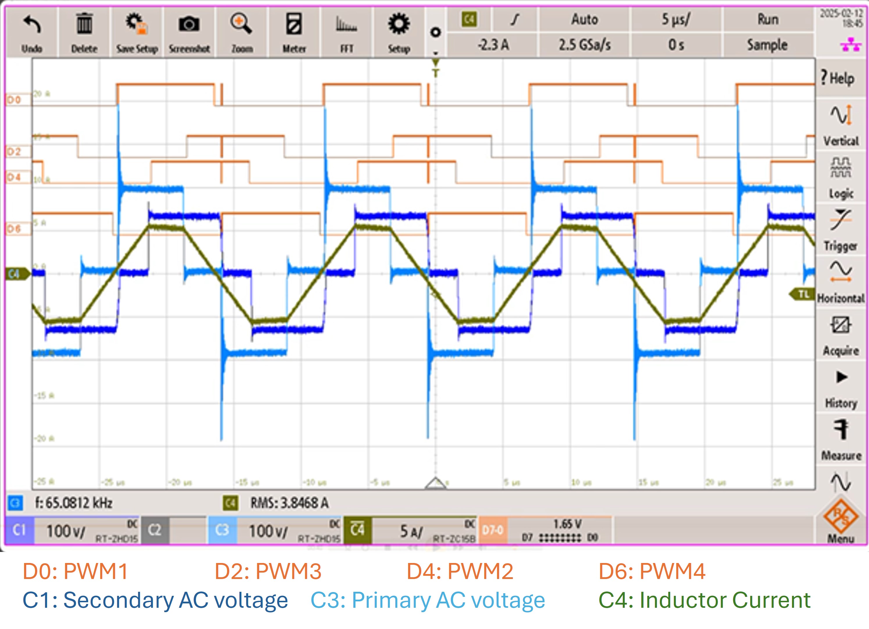
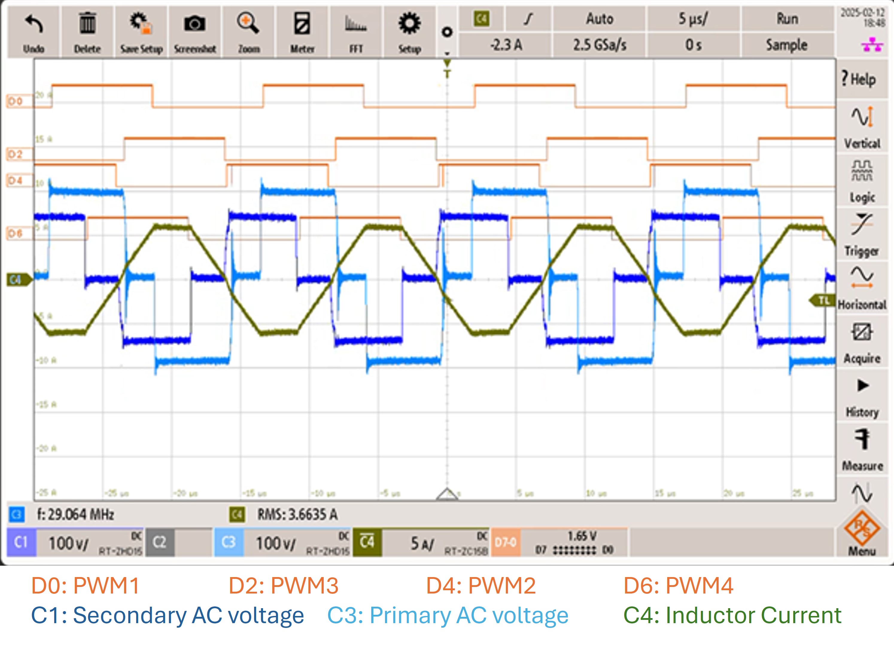
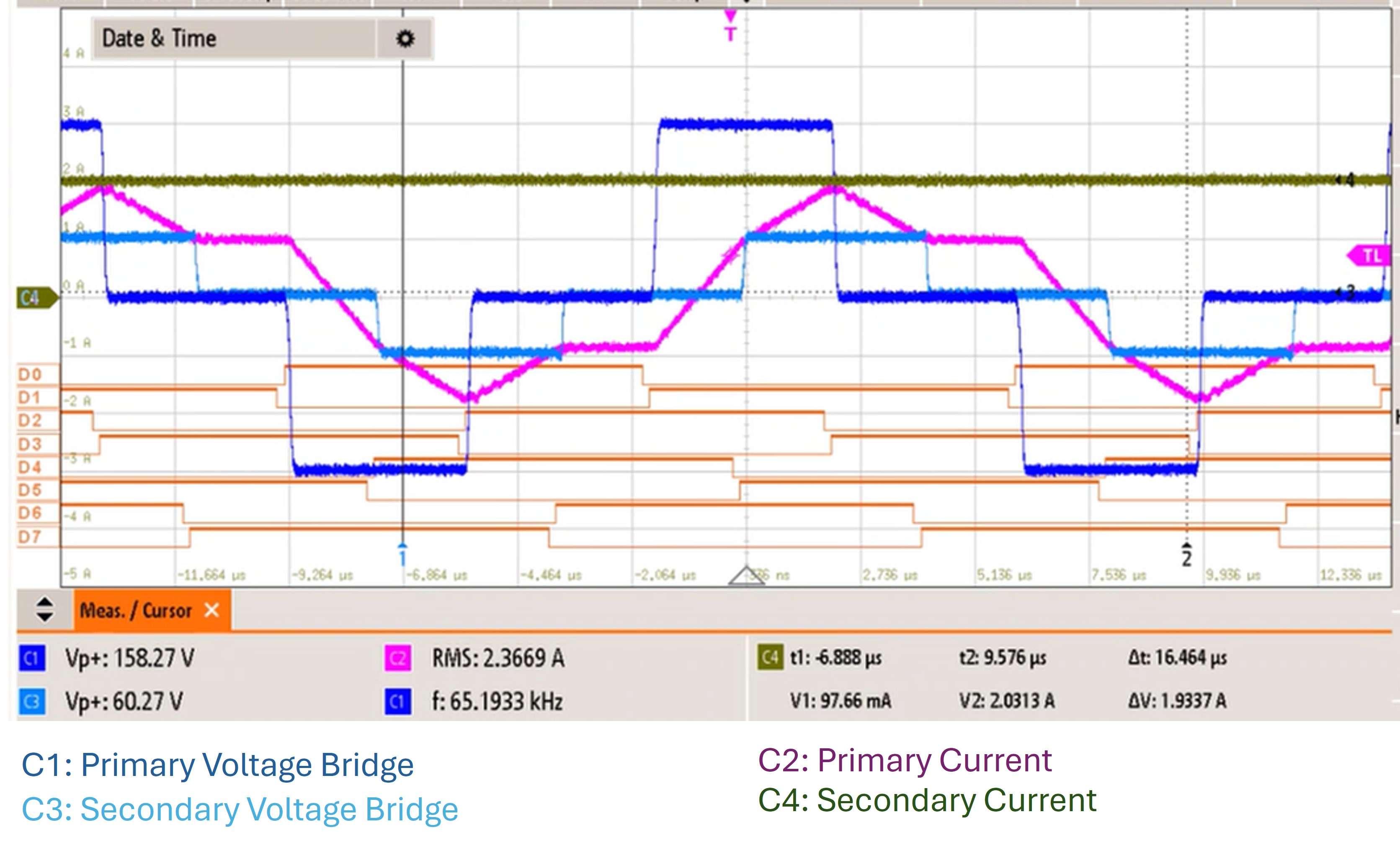
In the figures below, a comparison of forward and reverse operation is shown. Observe the 180� phase difference in the current waveform, which translates to positive or negative active power flow.
When transitioning the mode of operation of the Dual Active Bridge (DAB) from forward to reverse, it is crucial to consider the voltage on the primary side. The isolated voltage sensing circuit, which is responsible for monitoring the primary side voltage, requires a voltage higher than 100V to function reliably. If the primary side voltage falls below this threshold, the circuit may not operate correctly, leading to unreliable performance and inaccurate voltage measurements.
To ensure the isolated voltage sensing circuit operates correctly, it is essential to maintain the primary side voltage above 100V. This voltage level is necessary for the proper powering of the circuit components specially the PIC16 device that detects the primary voltage.
Additionally, when initiating the reverse mode operation, a careful ramp-up sequence must be followed. This precaution is necessary to prevent dangerous voltage overshoots, which can occur if the voltage increases too rapidly.
By adhering to a controlled ramp-up procedure, the system can gradually adjust to the reverse mode, ensuring stable and safe operation. This involves managing the slew rate of the voltage increase to avoid sudden spikes that could result in overshoot. Proper ramp control is critical for maintaining the integrity and safety of the system during mode transitions.
The main power controller state machine, executed every 100 microseconds, is detailed in the function Dev_PwrCtrl_StateMachine(POWER_CONTROL_t* pcInstance) located in pwrctrl/pwrctrl_sm.c. The state machine progresses through a series of steps in a specific chronological order during its execution.
The state machine for the power control system (PCS) operates as follows:
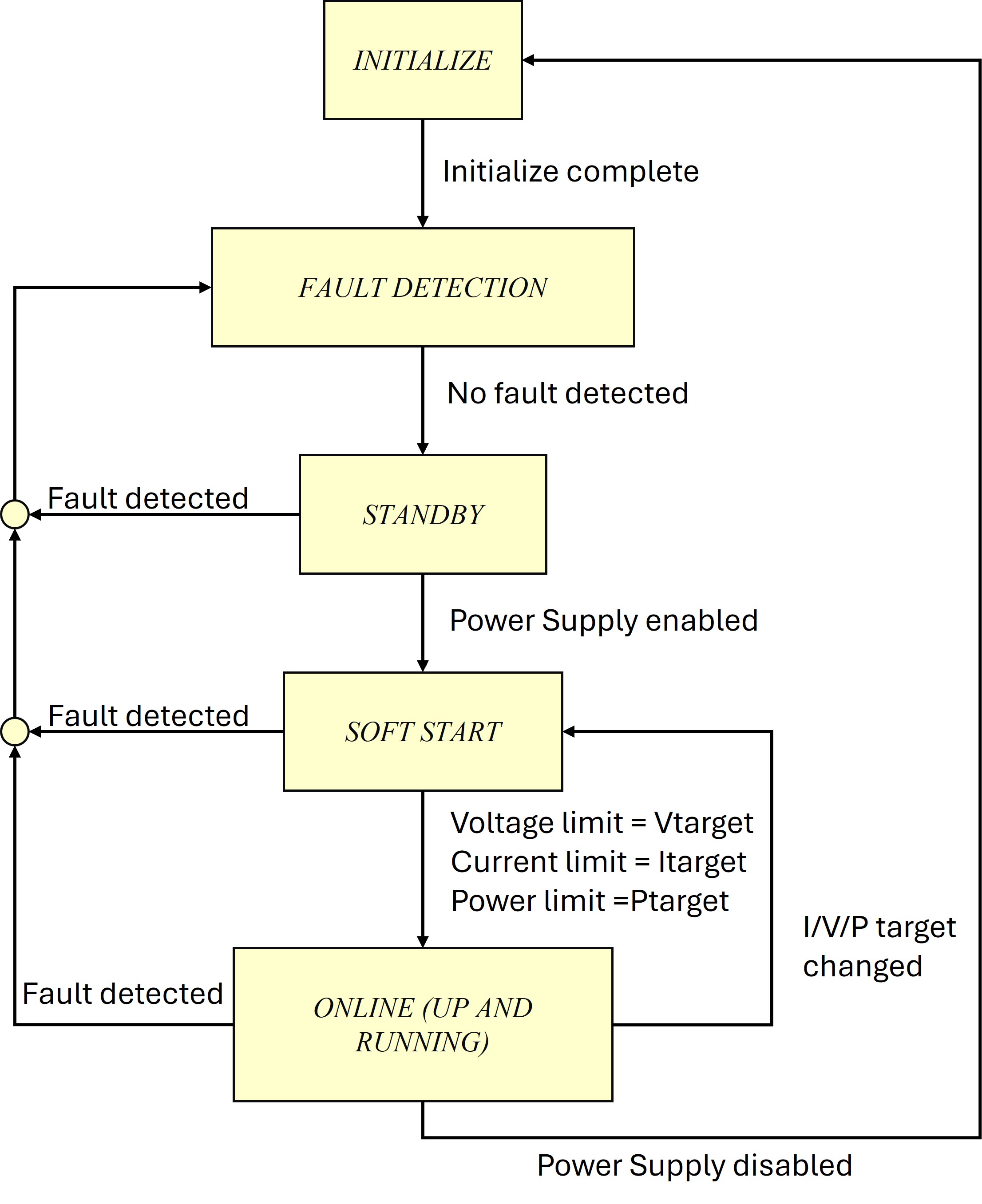
Before utilizing the state machine, it is essential to define and initialize at least one Power control data object within the power control code. The following outlines the data structure of POWER_CONTROL_t and its usage.
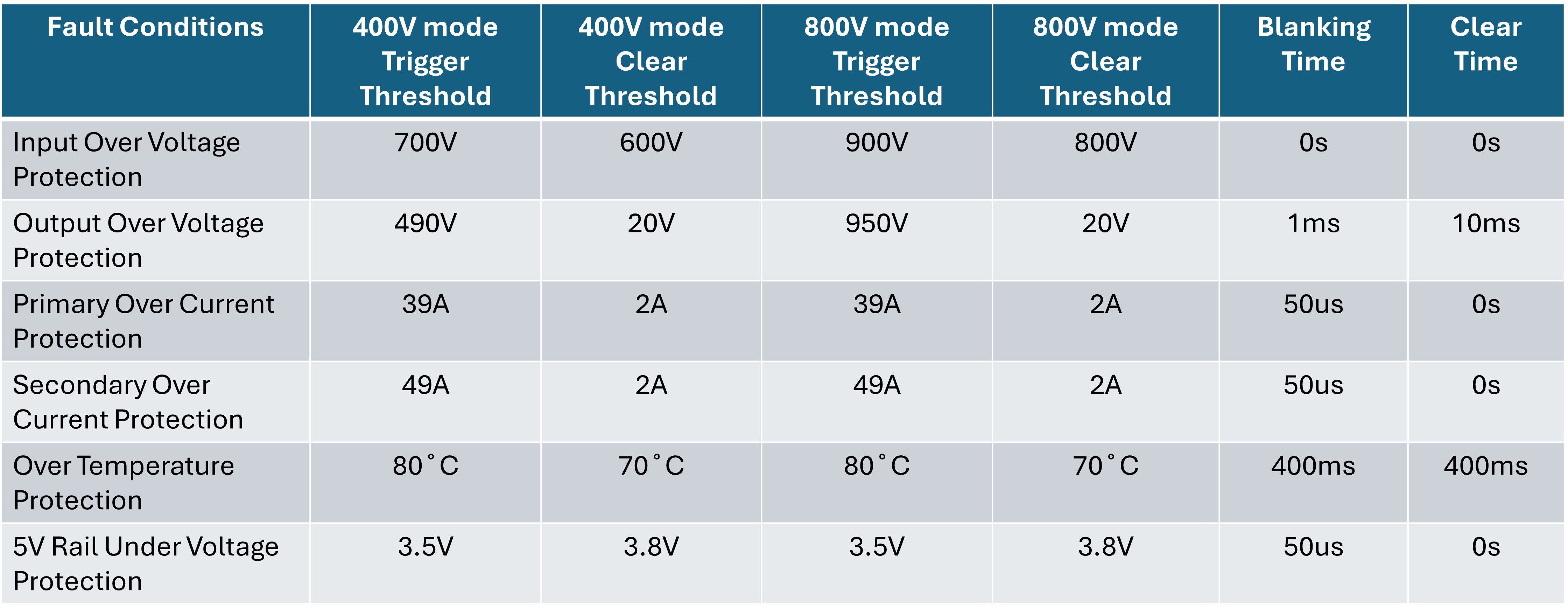
The fault protection code, executed every 10 microseconds within the interrupt service routine in the function Dev_Fault_Execute(), is located in the file fault/fault.c. There are two types of protection: firmware fault protection, implemented on the dsPIC on the DP-PIM, and hardware fault protection, implemented on the DAB power board. The primary purpose of these protections is to prevent catastrophic board damage, especially from input and output overcurrent events.
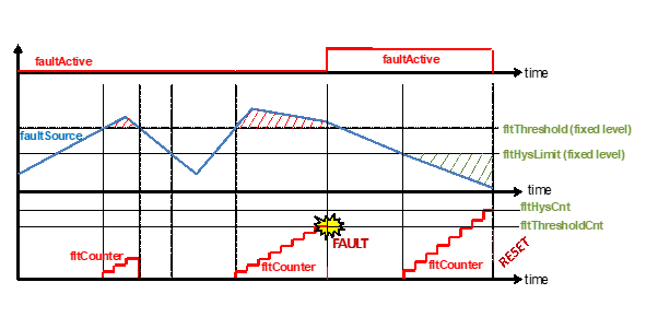
All our firmware fault protection systems operate with the same functionality, incorporating a trigger threshold, a clear threshold, a fault blanking time, and a fault clear time.
For instance, in the case of a fault with a "max" threshold (e.g., output over-voltage protection), the fault is triggered when the source exceeds the threshold. A timer starts once this threshold is breached. If the source remains above the threshold beyond the fault blanking time, the fault becomes active, causing the PWMs to switch off and the converter to enter the "FAULT ACTIVE" state. If the source drops below the threshold before the blanking time expires, the timer resets.
When the fault is active, it will be cleared if the source stays below the clear threshold for the fault clear time. Once all faults are cleared, the converter will either restart or be ready to start again.
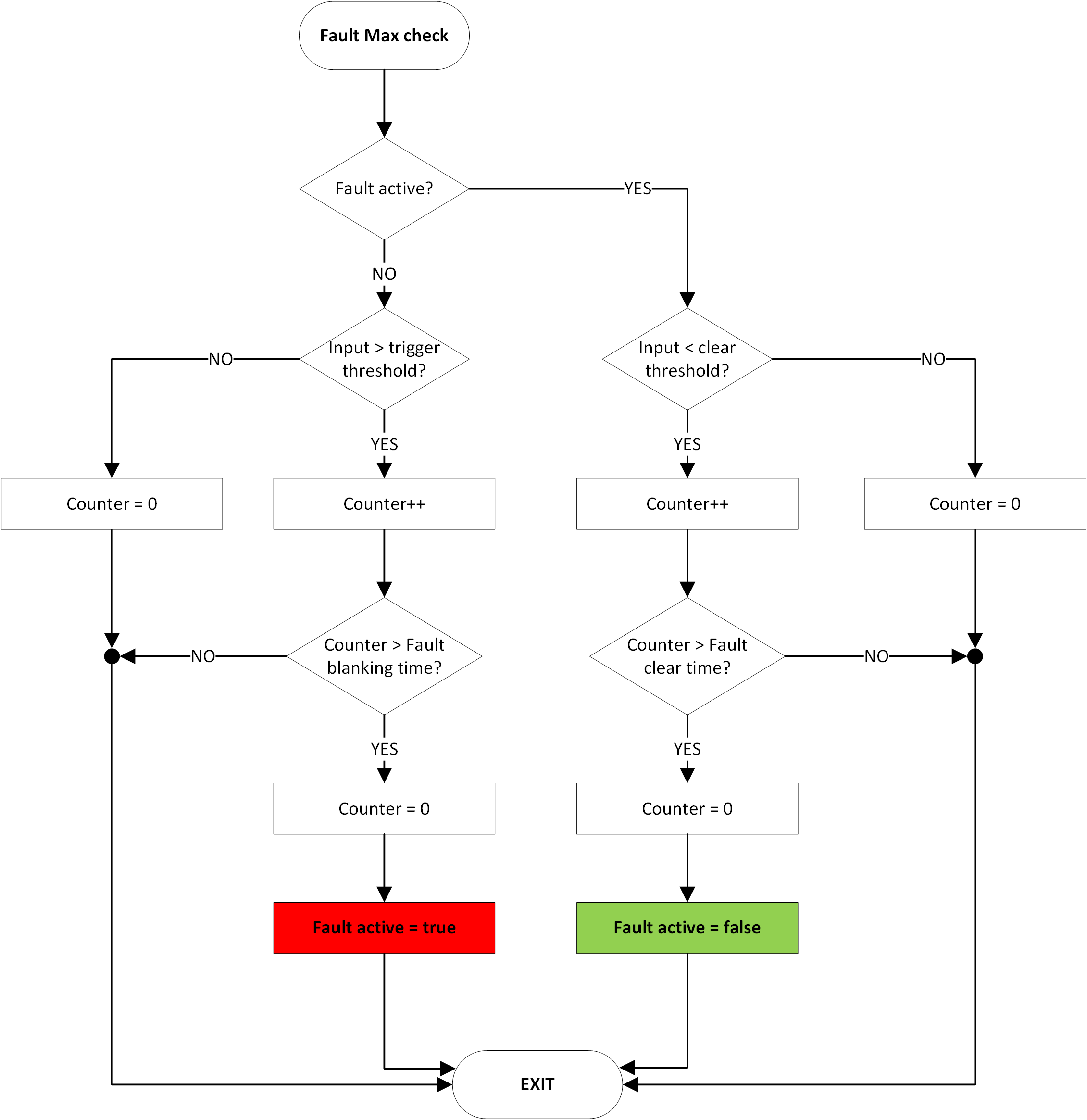
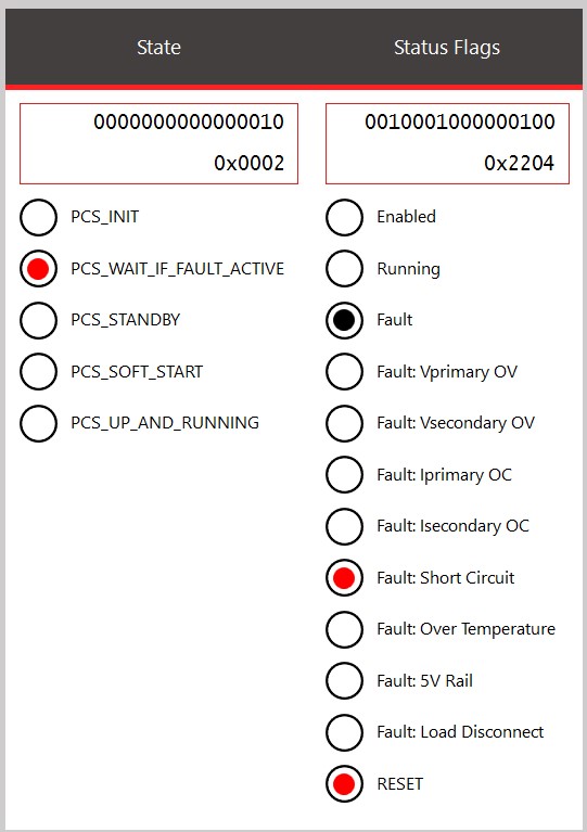
The accompanying flowchart illustrates the process in detail. If "fault active" is true, the fault is active, and the converter is disabled. Conversely, if "fault active" is false, the converter is permitted to attempt startup.
The table below lists all faults that are protected by our firmware, which executes fault protection every 10 microseconds.
The hardware fault protection system is engineered to avert significant board damage, particularly from input or output overcurrent. It activates instantaneously, setting all PWM drive signals to zero and shutting down the converter. This system functions independently of the dsPIC, ensuring that any drive signals from the dsPIC are overridden by the hardware protection before reaching the FET drivers.
When the hardware fault protection is triggered, it latches, meaning it will not reset automatically and requires manual intervention to clear.
To restart the board, there is a need to disable all PWMs by either removing the input supply or erasing the dsPIC firmware (the latter is recommended for safety).
The dsPIC implements output overcurrent protection using comparators and DACs as follows:
These comparators has built-in digital filter that could blank the unwanted comparator output transitions due to analog comparator input signals that has been corrupted by the large electromagnetic fields generated by the external switching power transistors.
If either comparator trips, it disable all PWM drive signals and placing the converter in the "FAULT ACTIVE" state. Since this is also a hardware fault protection, this fault protection is also latched, necessitating a dsPIC reset to restart the converter. If this fault protection is activated, the RESET flag in the Power Board Visualizer GUI will be set, indicating that the dsPIC needs to be reset to restart the DAB converter.
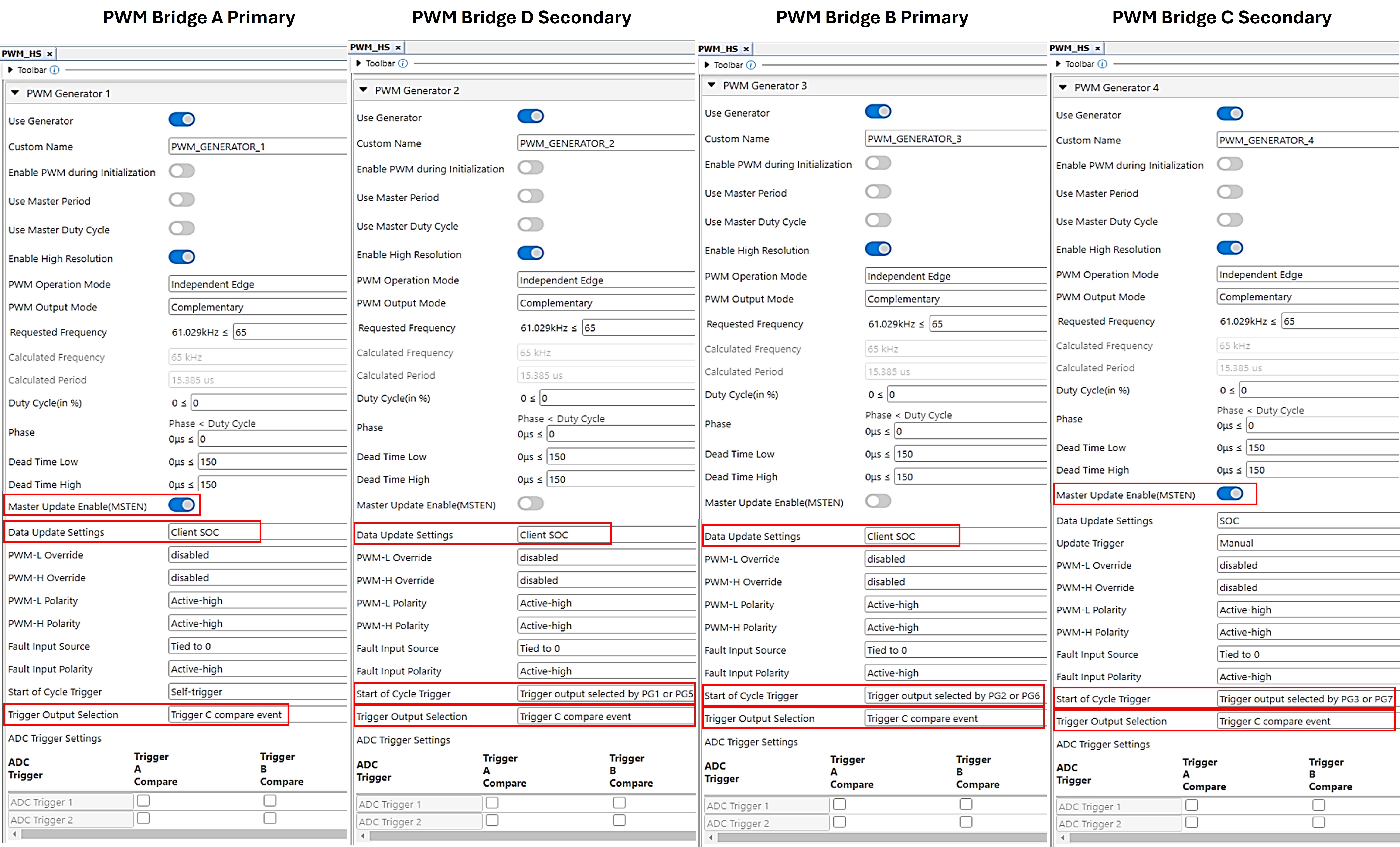
The PWM setup for the DAB application is primarily configured using MCC-generated initialization functions in the main function, with additional custom configurations applied as needed. The application employs a dual phase shift (DPS) modulation scheme, which adjusts the phases in both primary and secondary bridges. This approach offers advantages over traditional phase shift (TPS) control by reducing current stress and enhancing system efficiency.
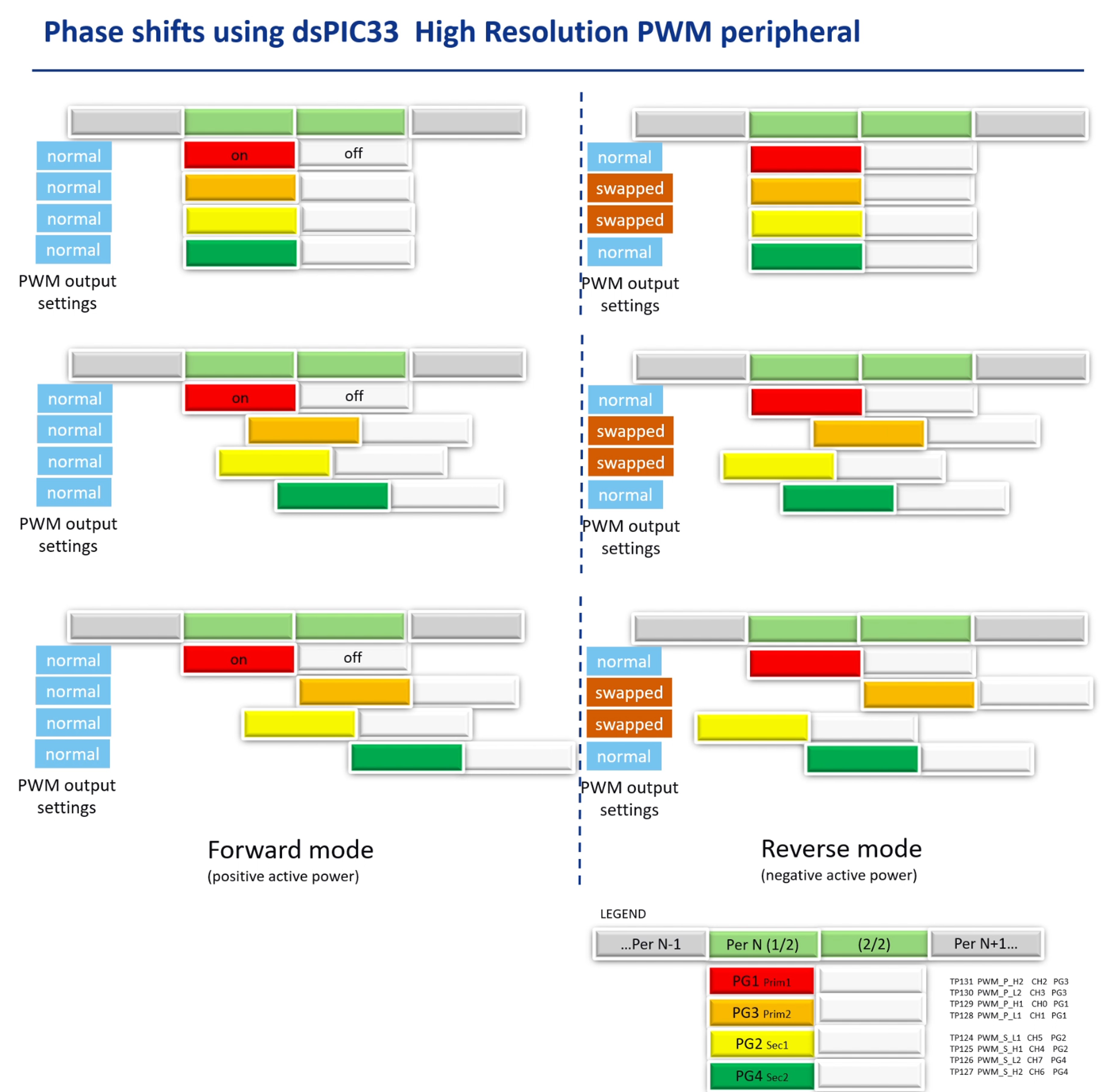
In this application, the primary bridge of the DAB is driven by PWM1 (for P1 and P2) and PWM3 (for P3 and P4), while the secondary bridge is driven by PWM2 (for S1 and S2) and PWM4 (for S3 and S4). Each PWM operates in complementary mode, with PWM3 and PWM4 having swapped outputs. The output swapping of the PWM is an additional PWM settings that can be found in driver/mcc_extension/drv_custom_config_pwm.h.
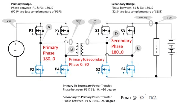
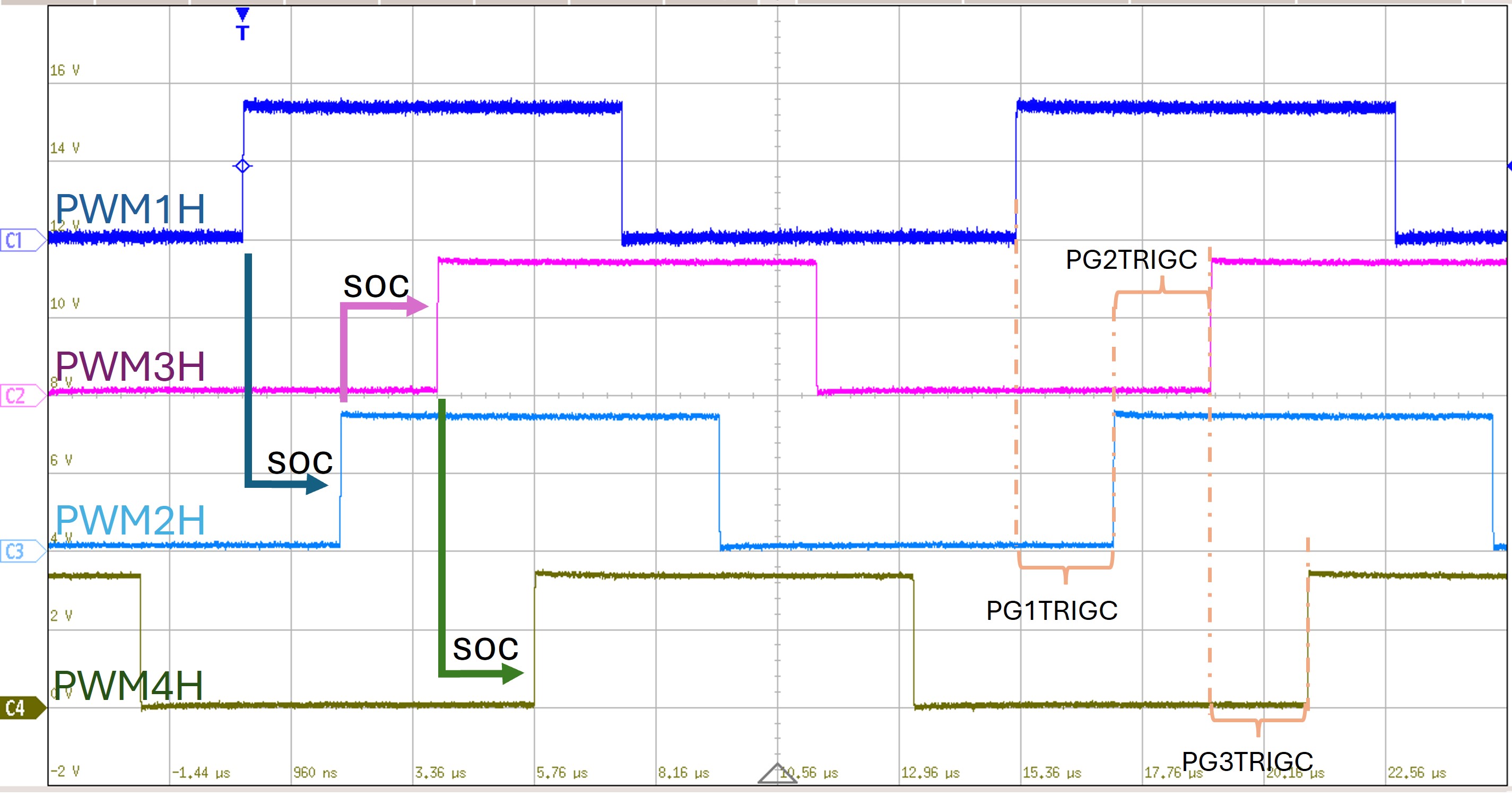
In a cascaded PWM configuration, the first PWM triggers subsequent PWMs in sequence, ensuring synchronized updates across all PWMs within the same cycle. In the DAB application, PWM1 acts as the master, while PWM2, PWM3, and PWM4 are secondary PWMs that follow PWM1. The configuration ensures that the start of each PWM cycle is dependent on the preceding PWM (e.g., PWM2 starts after PWM1, PWM3 after PWM2, and PWM4 after PWM3). PWM4, being the last in the sequence, broadcasts the update signal to all PWMs, ensuring synchronized data updates.
In the forward mode of the DAB converter, the PWM signals are configured to control the power flow from the primary side to the secondary side. In reverse mode, the power flow is reversed, going from the secondary side back to the primary side. This reversal requires a different configuration of the PWM signals to ensure proper operation. Specifically, for proper control in reverse mode, the complementary outputs of PWM2 and PWM3 need to be swapped. This means that the signal originally output on PWM2H in forward mode should now be output on PWM2L, and vice versa. This swapping ensures that the switching sequence of the transistors is correct for the reverse power flow. The figure below shows how the PWM works from no power to full power operation for both forward and reverse operating mode.
In this project, the Microchip Digital Compensator Design Tool has been employed for managing control loops. This software utility is specifically designed to aid engineers in the development and optimization of digital compensators for power supply systems. The tool streamlines the design process of digital control loops by offering an intuitive interface for configuring and tuning compensators.
This tool generates control loop files that are essential for code development. These files can be found in the directory pwrctrl/dcdt/. In the file pwrctrl_dcdt.c, users need to initialize the A- and B- coefficients of the control loop from DCDT, as well as set the scaling and limits for the control loop output. The control loop compensator is executed within the control loop interrupt service routine. This application includes three compensators: Voltage Loop, Current Loop, and Power Loop. The compensators are configured to allow users to adjust their limits in the Power Board Visualizer. The compensator with the lowest reference threshold will take precedence in controlling the loop.
Each mode of operation of the DAB (forward/reverse) features distinct control loops for voltage, current, and power.
Charging Direction:
Discharge Direction:
© 2025, Microchip Technology Inc.