An overview of the firmware is shown below. The power controller state machine and fault handler are executed every 100us by the scheduler. So also are the GUI handler (every 1ms), and the HMI driver (every 100ms).
There are 5 interrupt sources.
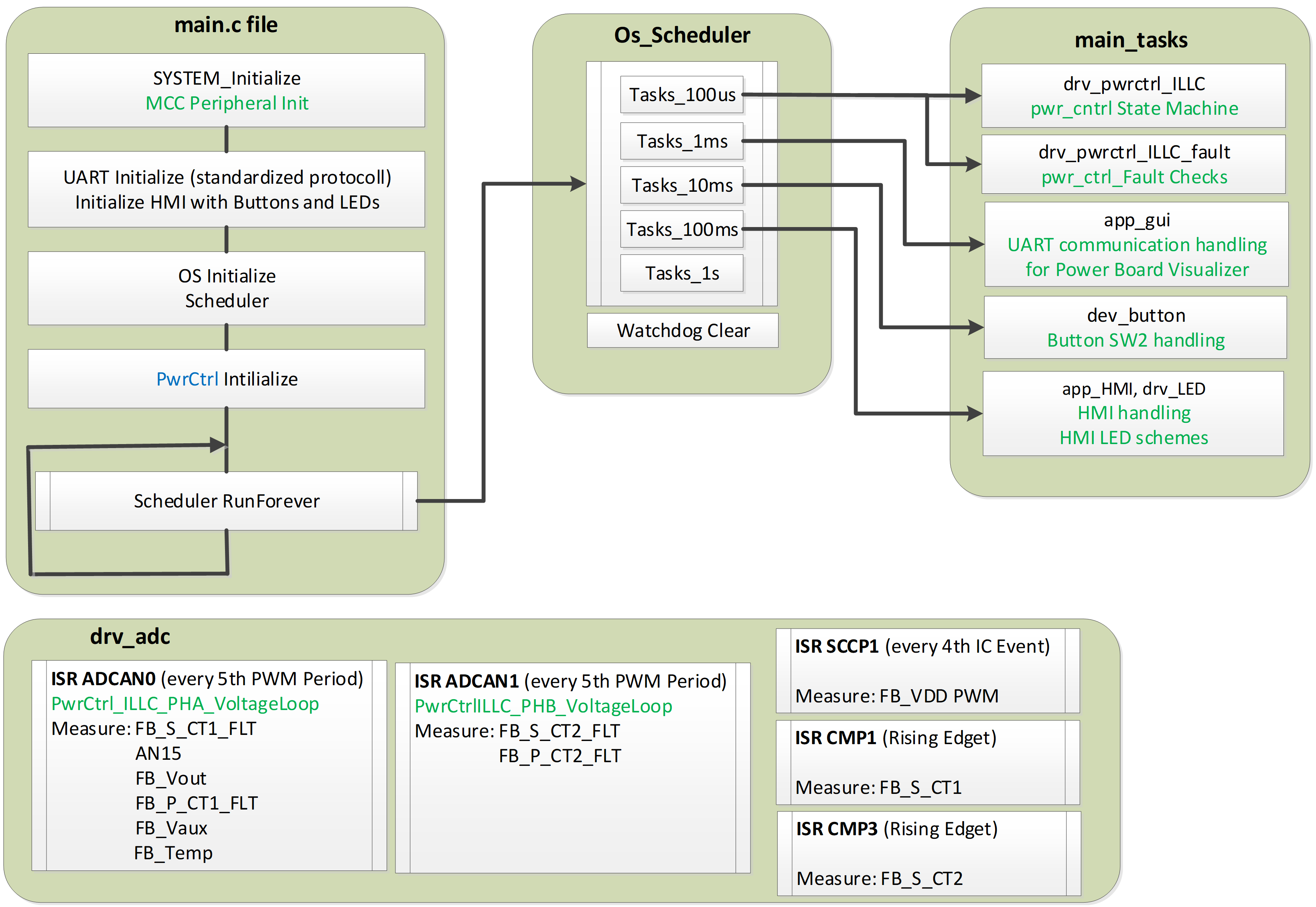
Microchip Code Configurator (MCC) is used to configure the peripherals. They are configured at run-time at the start of main(), before the background loop is initiated.
The main files are as follows:
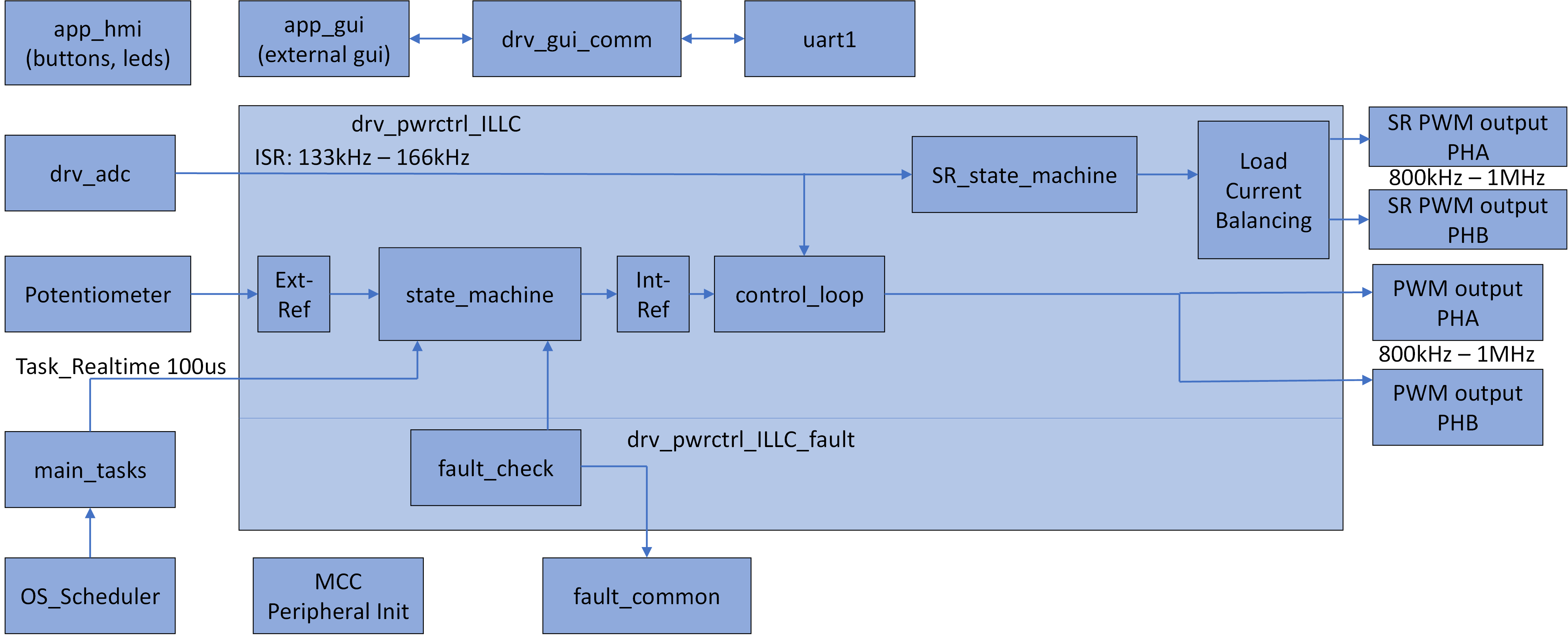
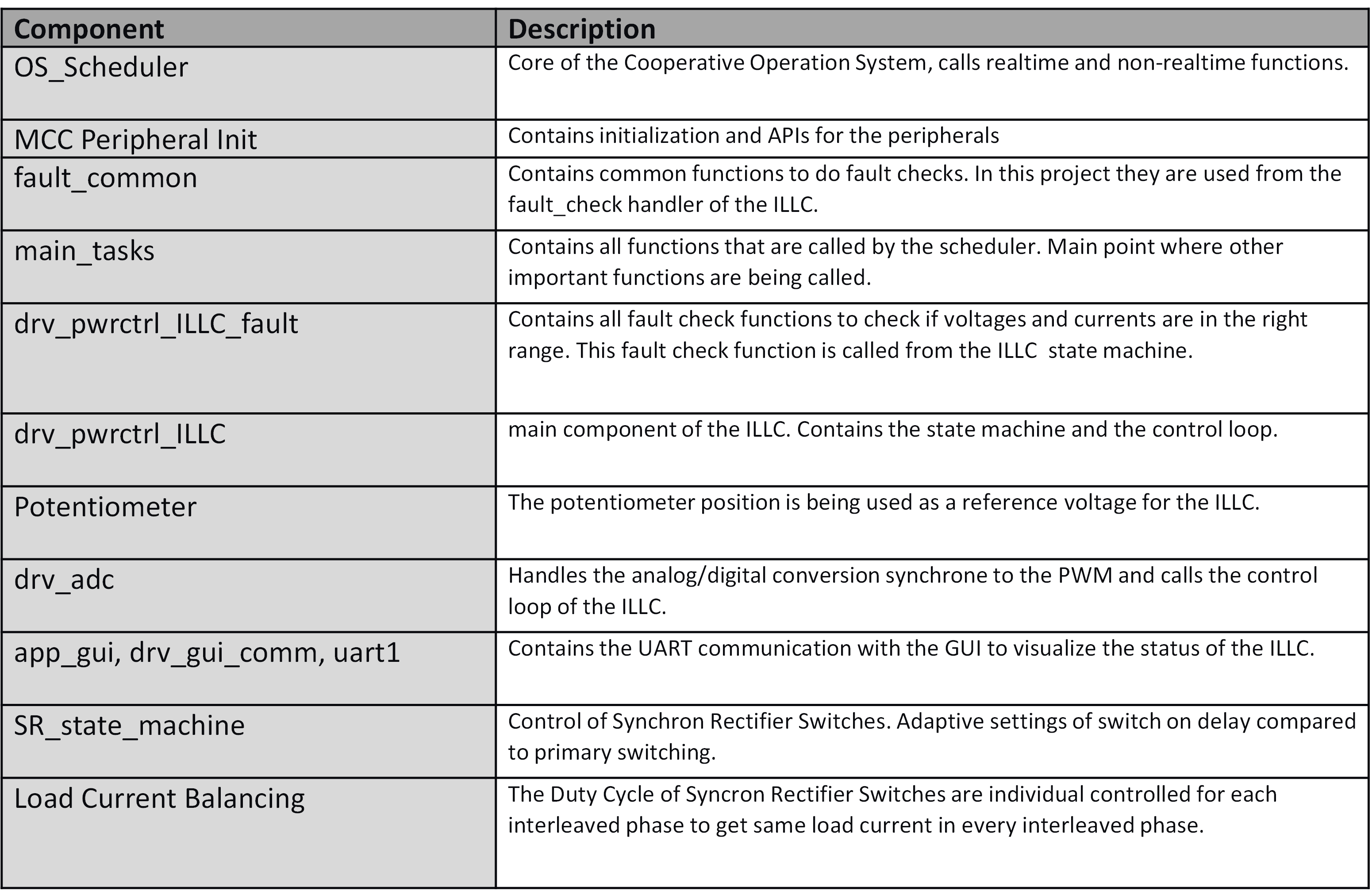
We now will go into more detail on certain parts of the firmware project that we deemed important and/or difficult to understand.
The LLC power board contains two phases, phase A and phase B. The firmware can be configured to run just a single phase (phase A), or run in interleaved mode (phase A and phase B both running).
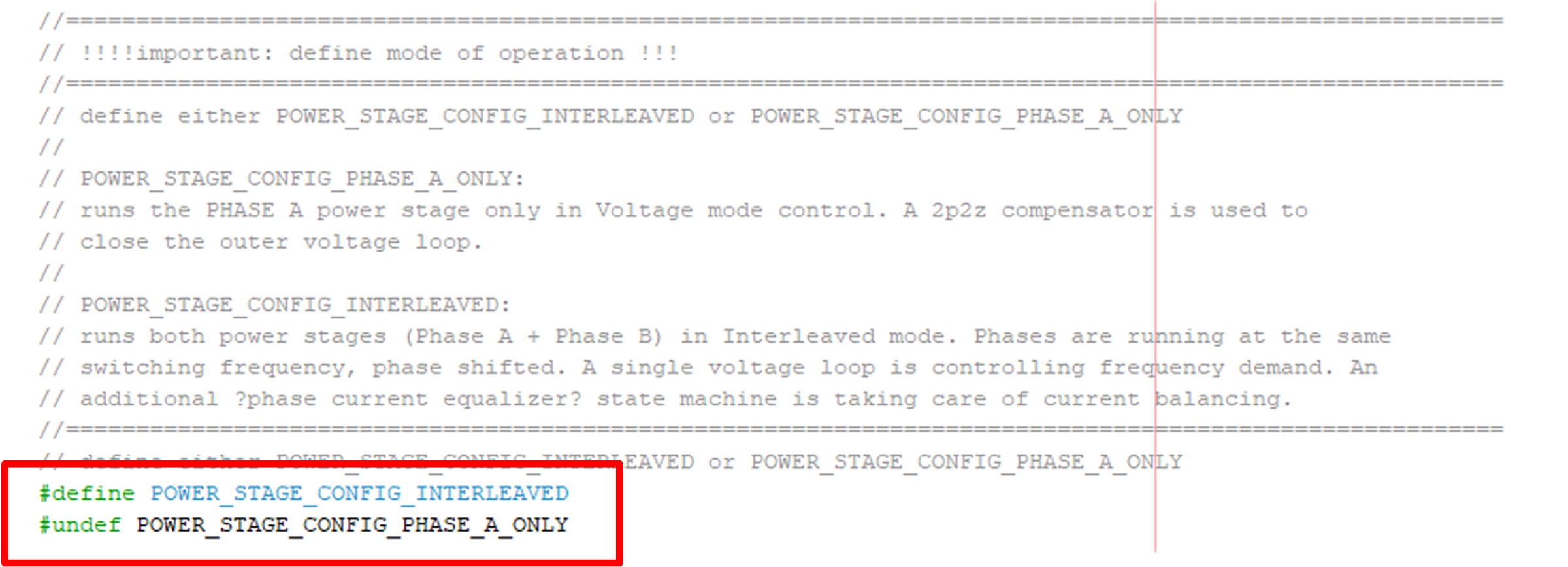
To configure the mode of operation, open the header file "project_settings.h".
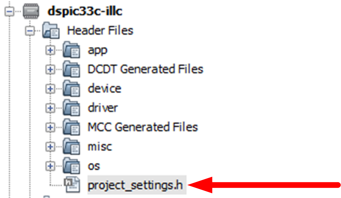
Scroll down to line 58 (see below).
To run in interleaved mode, POWER_STAGE_CONFIG_INTERLEAVED needs to be defined and POWER_STAGE_CONFIG_PHASE_A_ONLY should not be defined.
To run in phase A only, POWER_STAGE_CONFIG_PHASE_A_ONLY needs to be defined and POWER_STAGE_CONFIG_INTERLEAVED should not be defined.
If neither or both are defined, you will get a compile error.
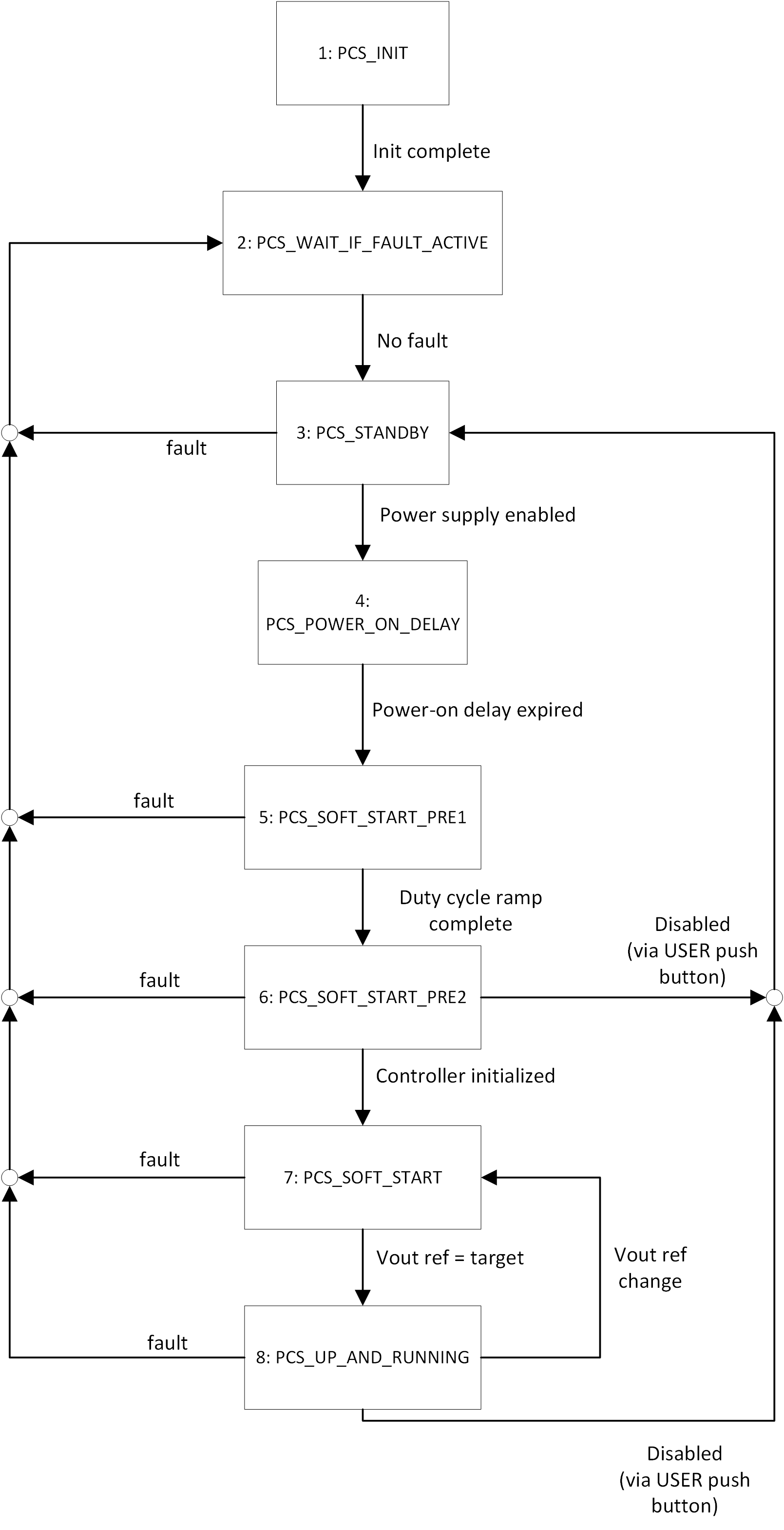
The main power controller state machine is illustrated below. It is executed every 100us. The code is located in power_controller/drv_pwrctrl_ILLC.c, see the function_Drv_PwrCtrl_ILLC_Task_100us()_. Most of the states are pretty standard for a digital DC/DC converter state machine (see state diagram below). Perhaps the only states worth describing in detail are the soft-start states, as these differ somewhat from other DC/DC converter state machines. Hence these are described in some detail below.
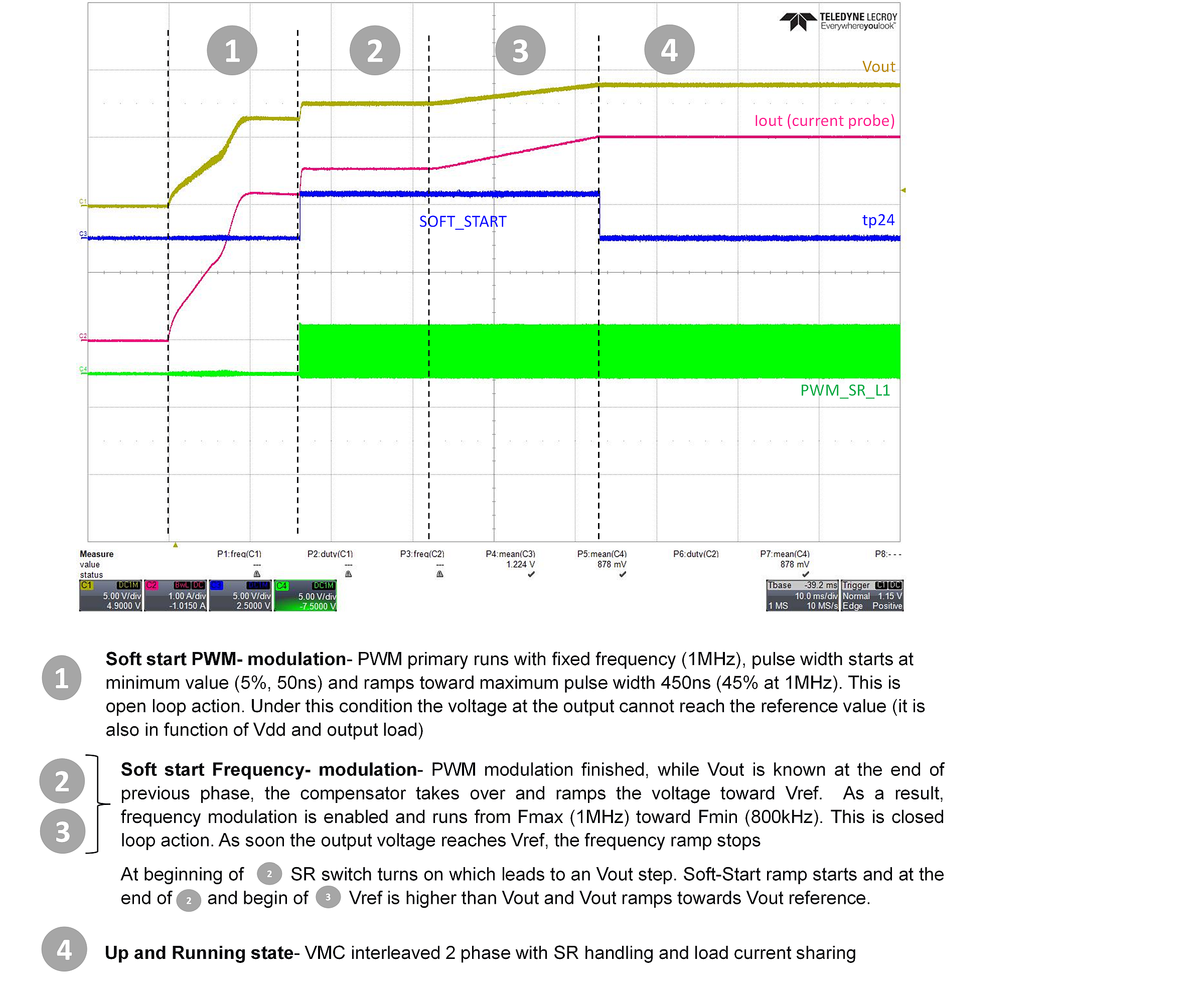
The soft-start ramp is split in 2 parts
(1) Run primary drive PWMs open-loop, at a fixed frequency of 1MHz (max frequency for our design)
(2) Run primary-drive PWMs closed-loop
Part 1 of the soft-start ramp is to prevent massive inrush current: if the duty cycle was set immediately to 50% the inrush current required to charge the output capacitor would trip the hardware over current protection. Thus part 1 is a duty cycle soft-start.
Note that the SRs drives (PWM2 for phase A and PWM4 for phase B) are switched off during soft-start, so any output current conduction is through the body diodes of the SRs during this time.
Also note that if we are running in interleaved mode, PG3 setup is identical to PG1, but PG3 lags PG1 by 90 degrees.
In this state, the PWMs are running in open-loop mode (that is, they are not driven by the compensator). The frequency is fixed at 1MHz. The on-time of the primary side half-bridge drive signals is set to 50ns. Then every 100us, the on-time (and hence duty cycle) is increase by 2.5ns. This continues until the duty cycle is 45% (as we allow for a dead-time of 50ns).
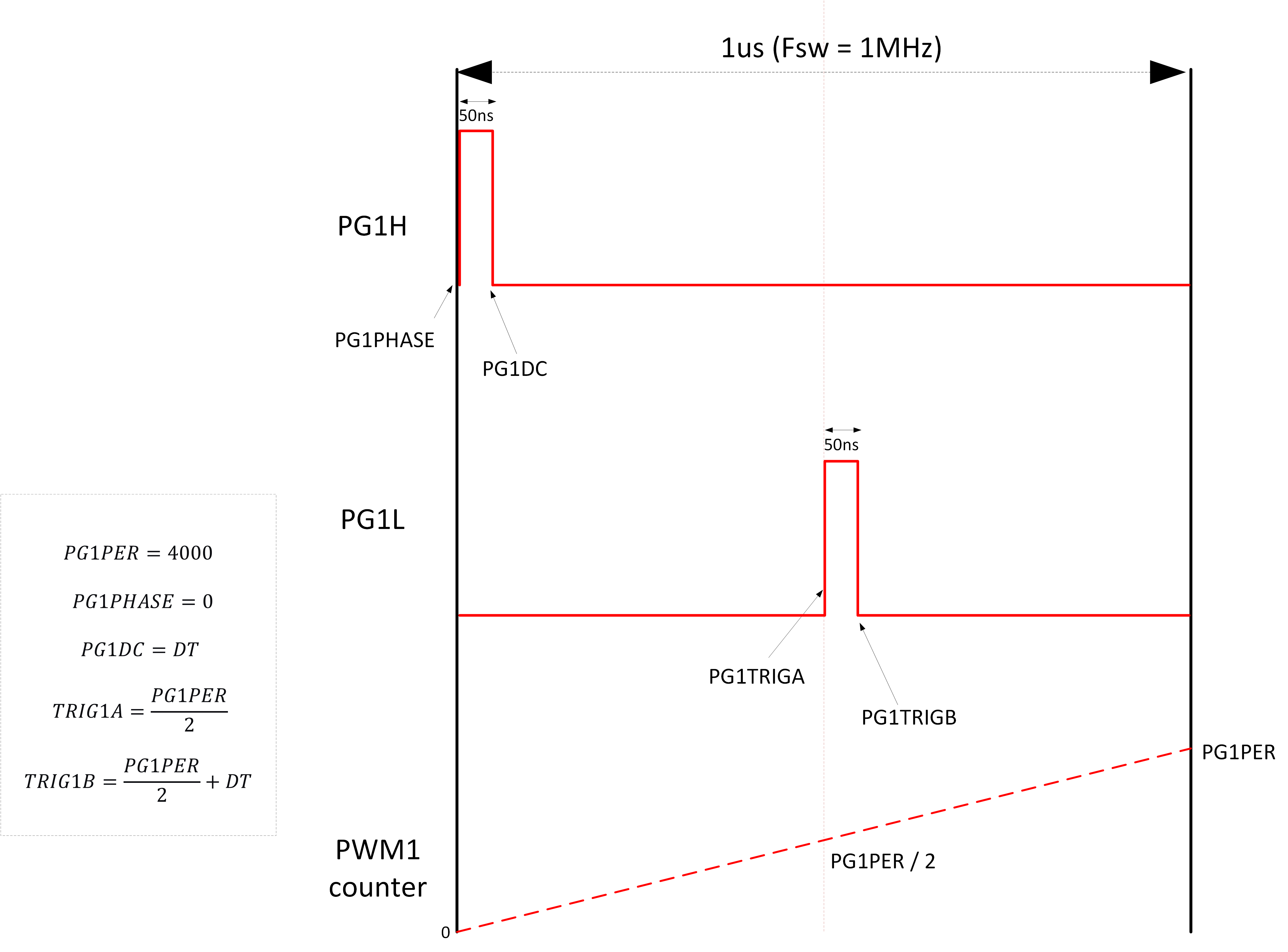
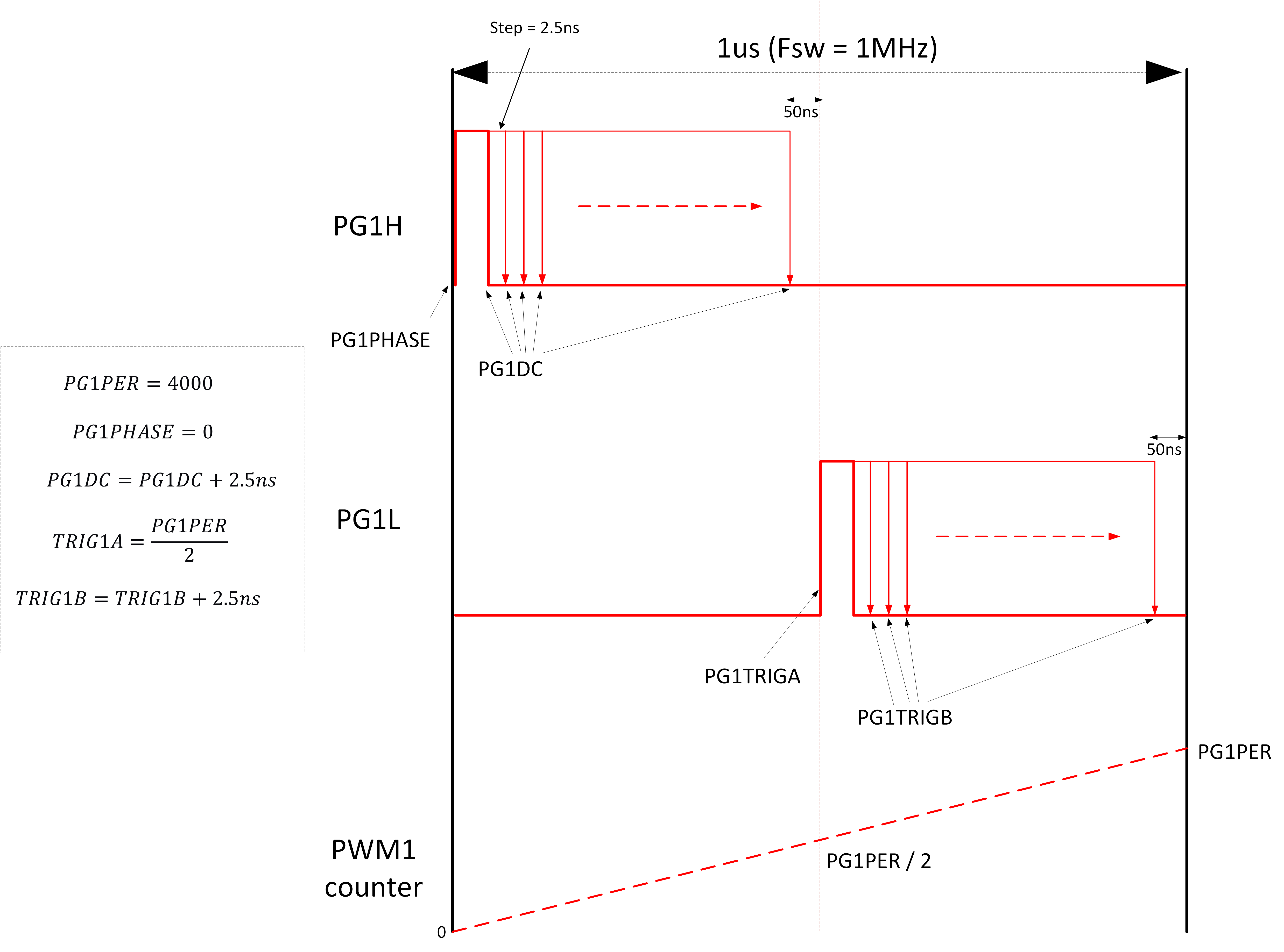
Once we reach the target primary drive on-time (equivalent to 45% duty cycle), we move to the state PCS_SOFT_START_PRE2.
In this state, we enable frequency modulation of the PWM outputs by the voltage mode compensator (closed-loop mode of operation). The on-time of the primary side PWM drive signals is fixed at (PG1PER/2 - 50ns). The voltage loop reference is initialized based on the measured output voltage at this point. Once we complete this initialization, we move to the state PCS_SOFT_START_.
In this state, the reference to the voltage loop compensator is ramped linearly to the target set-point. The compensator controls the frequency of the primary side LLC half-bridge signals. The duty cycle is always set to (PG1PER/2 - 50ns).
Note that in this state the SRs are enabled.
A oscilloscope screenshot of the entire start up phase is shown below. The different parts are described also.
The fault protection code is executed every 100us at the start of the converter state machine in the function Drv_PwrCtrl_ILLC_Fault_Check(). The body of the fault code is located in the files power_controller/drv_pwr_ctrl_ILLC_fault.c_and_misc/fault_common.c.
There are two types of protection:
The firmware fault protection is implemented on the dsPIC on the DP-PIM. The hardware fault protection is implemented on the LLC power board. It's purpose is to prevent catastrophic board damage, particularly due to input and output over current events.
All of our firmware fault protection has the same functionality. Each fault has a trigger threshold, a clear threshold, a fault blanking time and a fault clear time.
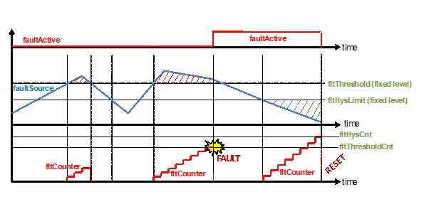
This is illustrated below, for a fault with a "max" threshold, which means that the fault is triggered when the fault source is above a threshold (output over voltage protection, for example).
Once the fault source breaches the trigger threshold, a timer is started. If the fault source stays above the trigger threshold for longer than the fault blanking time, then the fault becomes active, which means that the PWMs are switched off and the converter state machine is set to the "FAULT ACTIVE" state.
If the fault source drops back below the trigger threshold before the fault blanking time has expired, the timer is reset.
When the fault is active, if the fault source stays below the fault clear threshold for the duration of the fault clear time, then the fault is cleared. When all fault sources are cleared, the converter will attempt to restart.
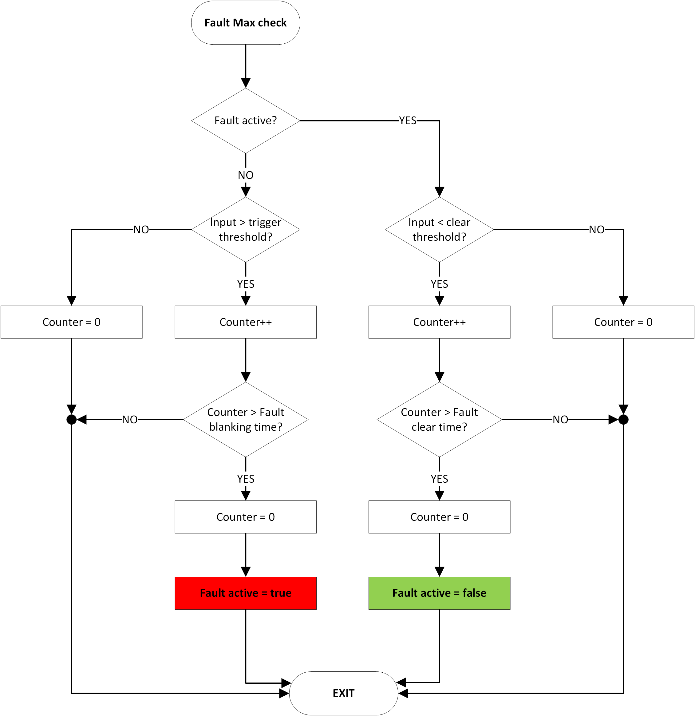
This is shown in more detail in a flowchart below. When "fault active == true", then the fault is active and the converter is disabled. When "fault active == false" the converter can attempt to start up.
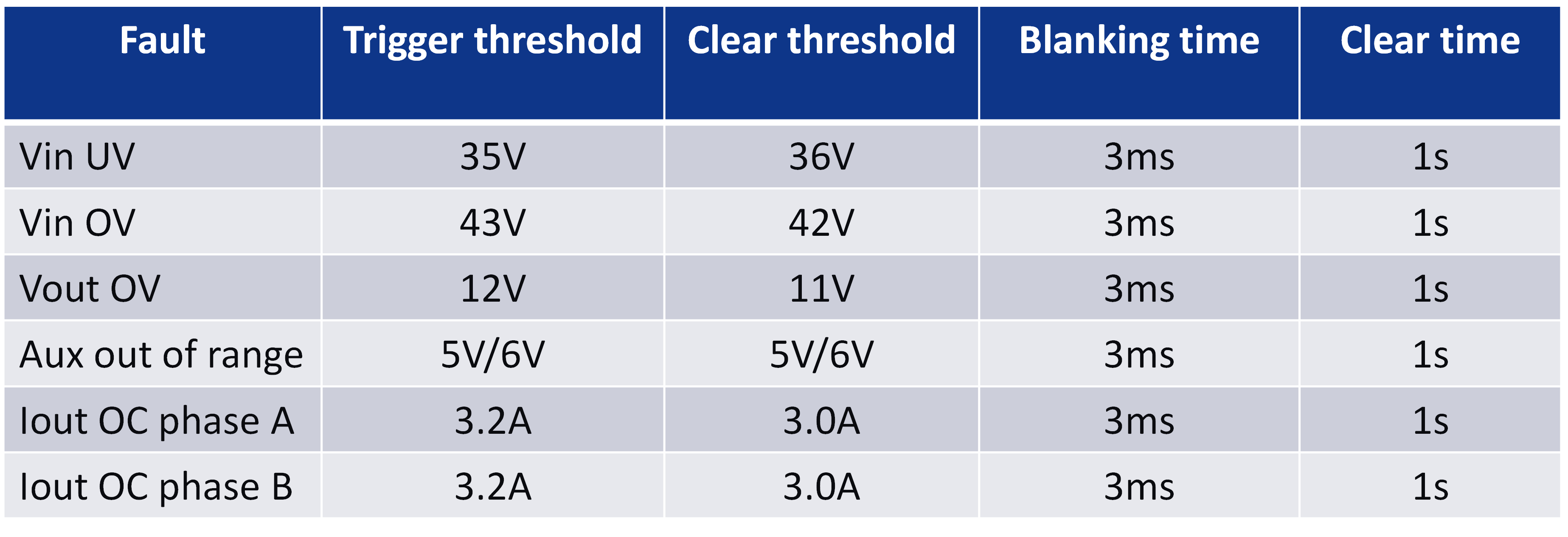
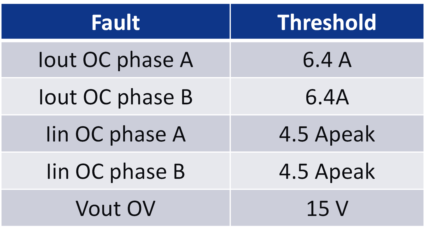
All faults shown in the table below have firmware protection like this. In our firmware, this fault protection is run every 100us.
The purpose of the hardware fault protection is to prevent catastrophic board damage, particularly from input or output over current. Once triggered, it kicks in immediately (there is no fault blanking time). It sets all PWM drive signals to 0, which will turn off the converter. Note that this is completely independent of the dsPIC, so even if there are drive signals coming from the dsPIC when the hardware fault protection is tripped, the hardware protection will over-ride these signals (through AND gates on the hardware) before they get to the FET drivers.
If the hardware fault protection is triggered, the red LED LD700 will turn on. The protection is latched, meaning that once triggered it will not clear itself, it needs to be manually cleared.
If you want to re-run the board, you need to
On the dsPIC, output over current protection using comparators and DACs is also implemented as follows:
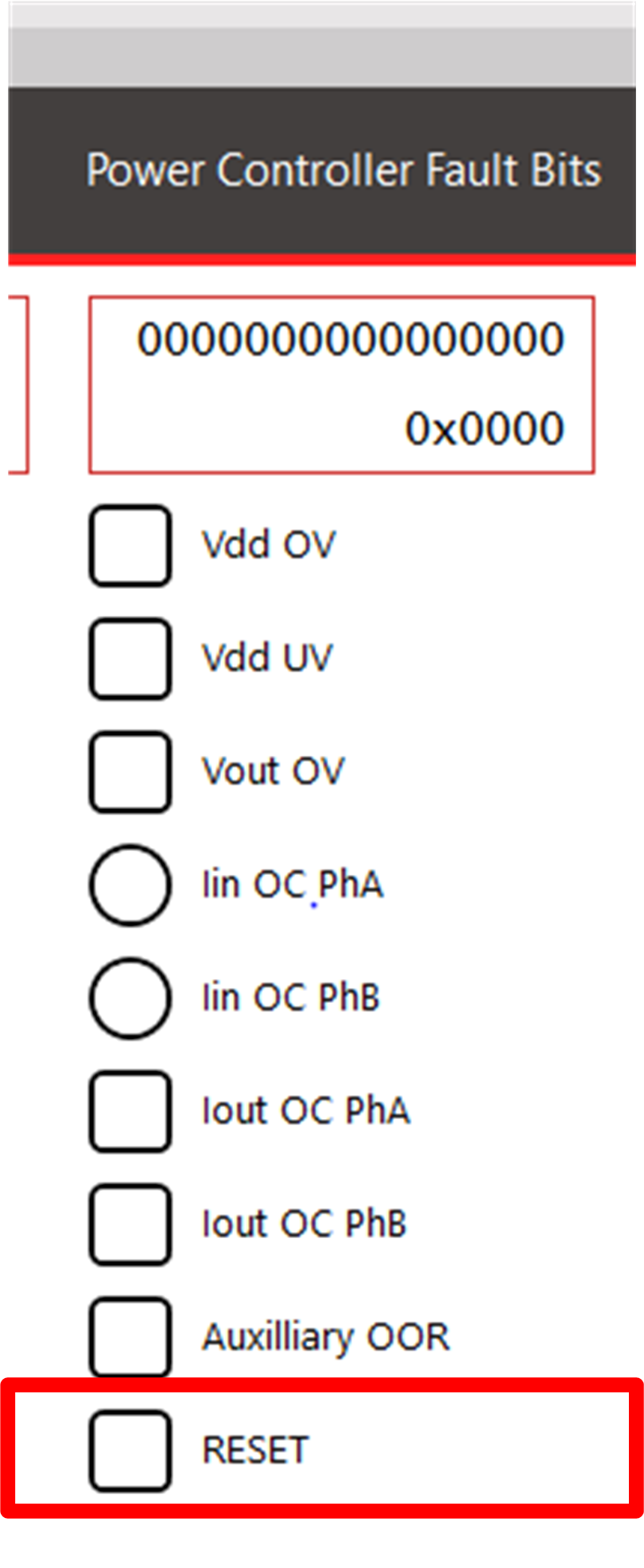
Either of these comparators tripping will trigger the highest priority interrupt, which disables all PWM drive signals and puts the converter in the "FAULT ACTIVE" state. Like the hardware fault protection, this fault protection is also latched, meaning that the dsPIC needs to be reset to restart the converter. If this fault protection is triggered, the RESET flag in the Power Board Visualizer GUI will be set, as shown below, indicating that the dsPIC needs to be reset to re-start the LLC converter.
Most of the PWM setup is done by calling initialization functions generated by MCC at the top of main(). Some more custom configuration is also done at runtime as required.
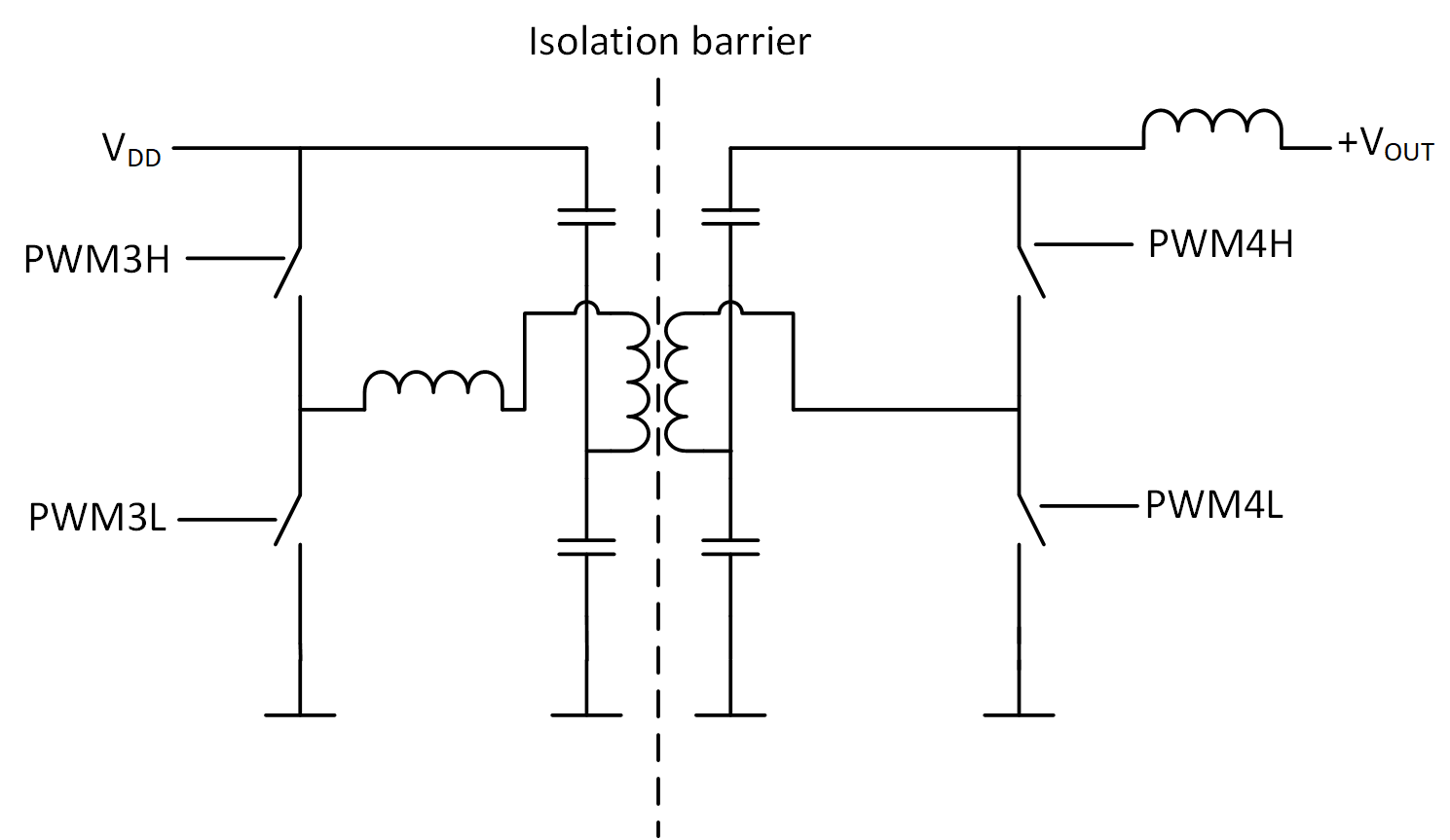
The two simplified schematics below show the routing of the PWM signals for phase A and phase B. PWM1 and PWM3 output are used for the primary drives for phase A and phase B respectively, while PWM2 and PWM4 are used for the SR drives.
The dsPIC is on the secondary side, so PWM1H, PWM1L, PWM3H and PWM3L have to pass through the isolation barrier. FET drivers are not shown here, please see the full schematic in the users guide for more detail.

The switching frequency range of our LLC solution is from 800kHz and 1MHz. To achieve robust operation in this frequency range with a PWM resolution of 250ps, we needed some special PWM module configuration, which will be describe in the following sections.
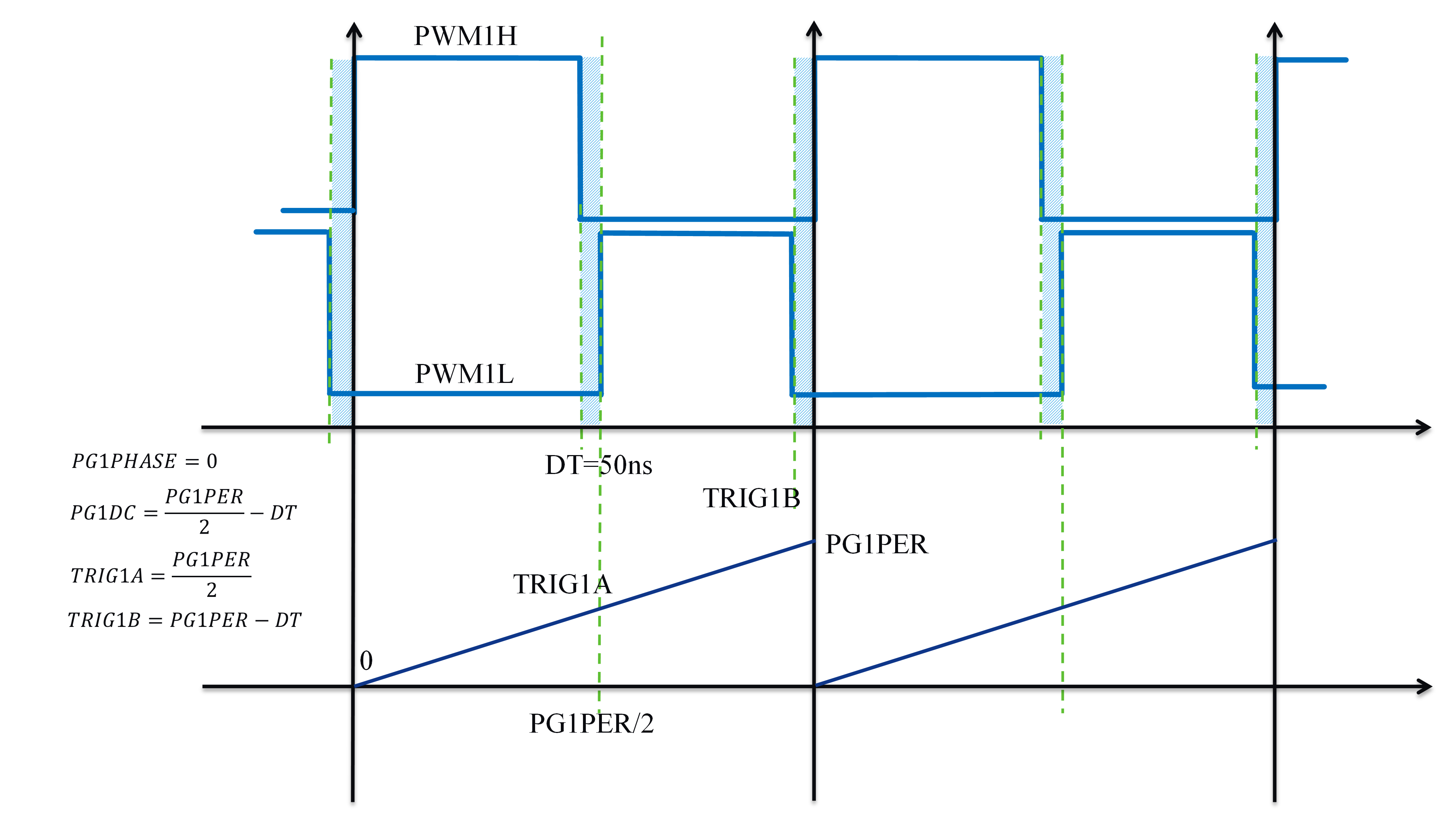
For a single phase, the LLC primary drive signals should have a fixed duty cycle (50% minus some dead time) and variable frequency, as shown below. The voltage loop compensator output modulates the switching frequency of the converter. The drive signals to the high side and low side of the primary side half-bridge (before the resonant tank) need to be complementary, with a dead time between the falling edge on the high side drive and the rising edge of the low side drive, and visa-versa.
In our example firmware, the frequency can cary from 800kHz (max output voltage) to 1MHz (min output voltage).
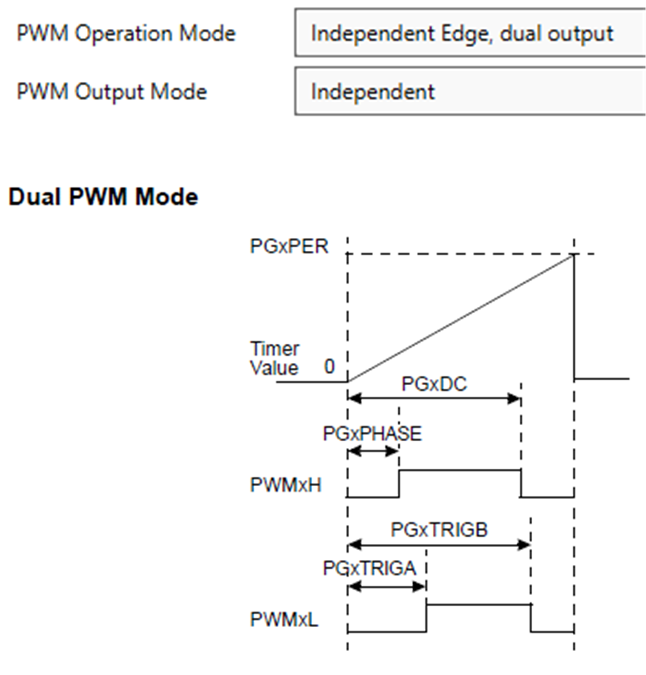
To get this type of waveform from the PWM module, we configured the PWM peripherals in "Independent Edge, dual output mode".
In this mode of operation, each PWM edge is set independently via a register. Specifically,
The primary drive signals for phase A (from PWM1 peripheral) are shown below.
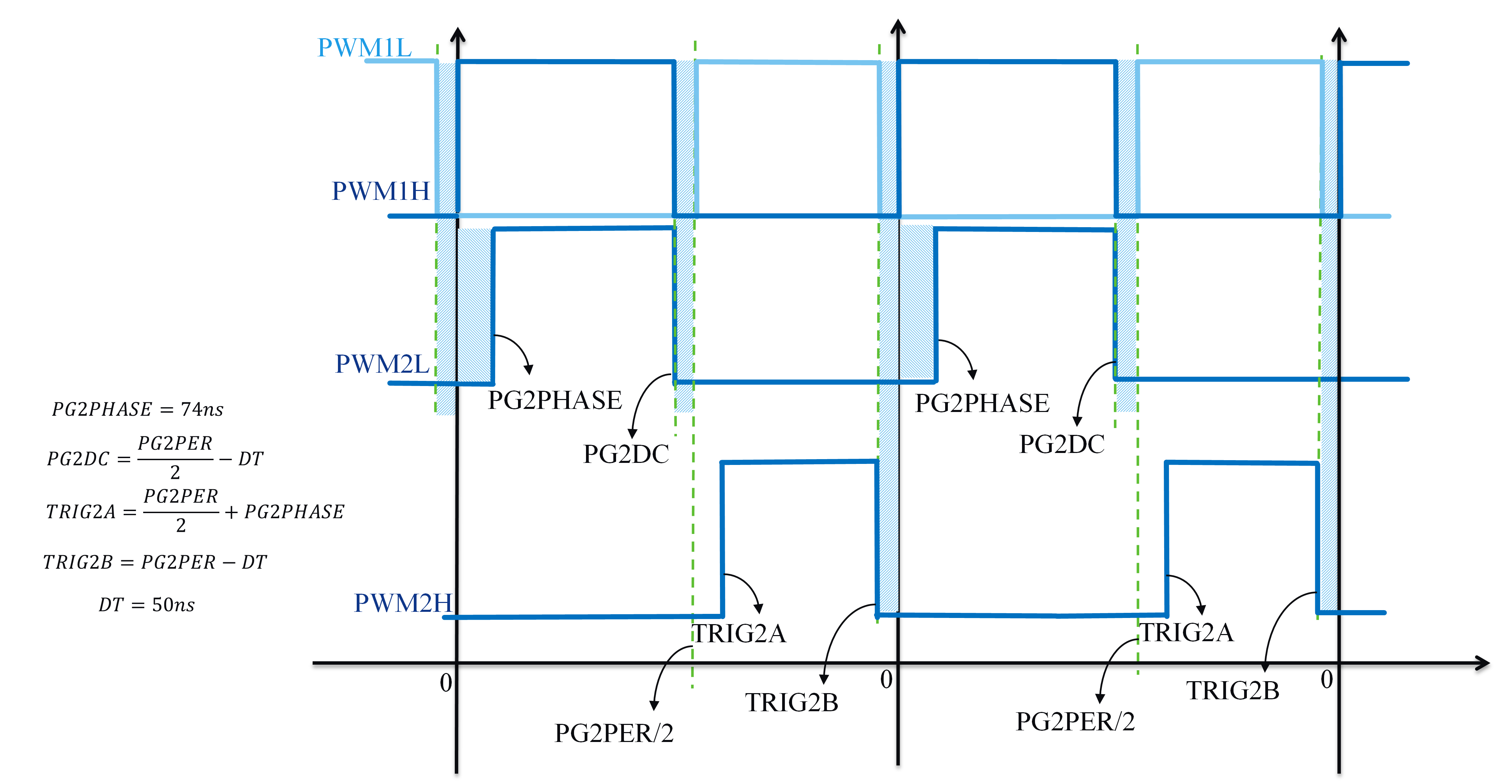
The SR drive signals for phase A come from the PWM2 module. PWM2H drives the SR on the high side of the half-bridge on the secondary side, and PWM2L drives the SR on the low-side. PWM2 is also configured in "independent edge, dual output" mode, but the SWAP bit is set, so that PWM2H and PWM2L are swapped. The PWM2H and PWM2L setup is illustrated below.
Phase B setup as follows:
Phase A and phase B run 90 degrees out of phase. The synchronization scheme works as follows:
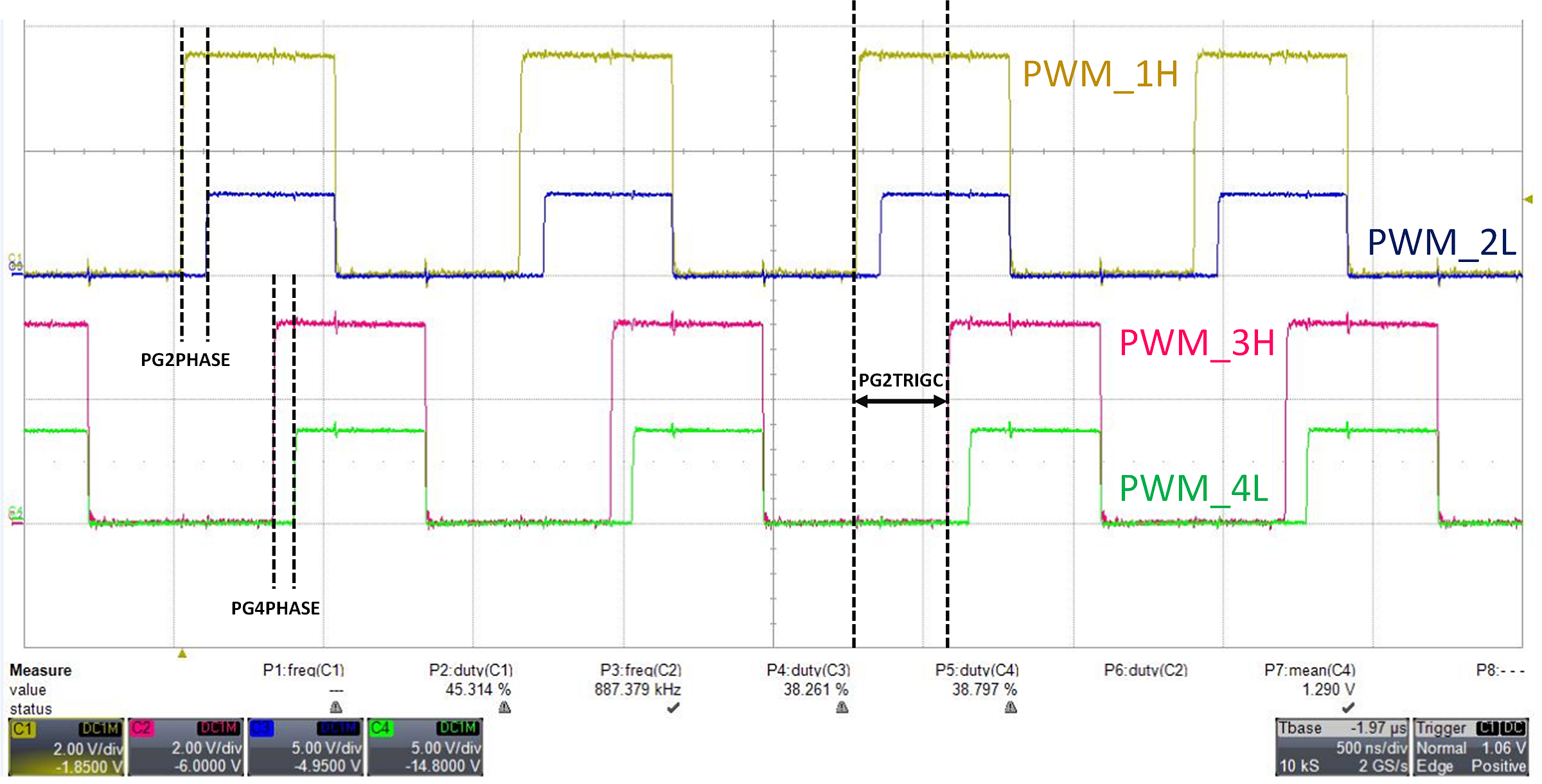
The ADC trigger for PWM1 is set to occur every 6th PWM1 period. It is set using PG1TRIGC (as PG1TRIGA and PG1TRIGB are already in use), and in the running firmware is set to be at the middle of the PG1H on-time so as to sample the average current.
The ADC trigger for PWM3 is set to occur every 6th PWM3 period. It is set using PG3TRIGC, and in the running firmware is set to be at the middle of the PG3H on-time so as to sample the average current.
The "easy setup" view for all 4 PWM modules is shown below.
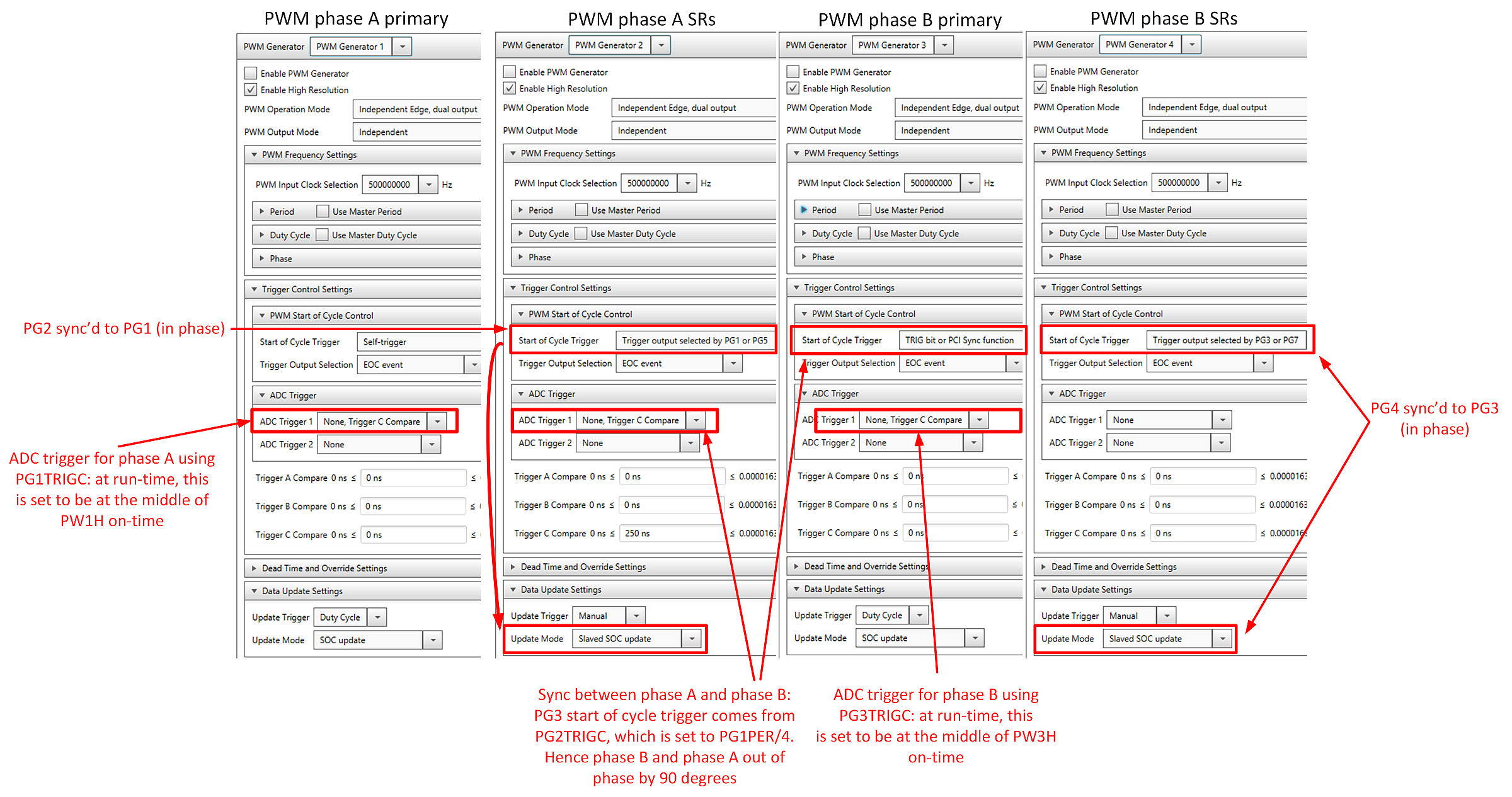
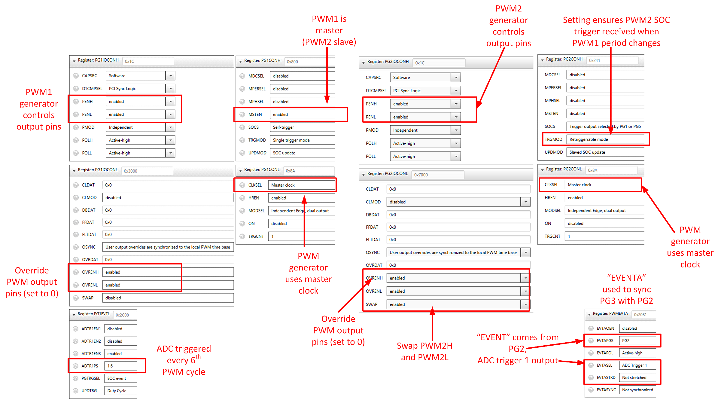
Some registers in the "registers" view also need to be modified. The fields that need to be modified for phase A (related to PWM1 and PWM2) are highlighted below.
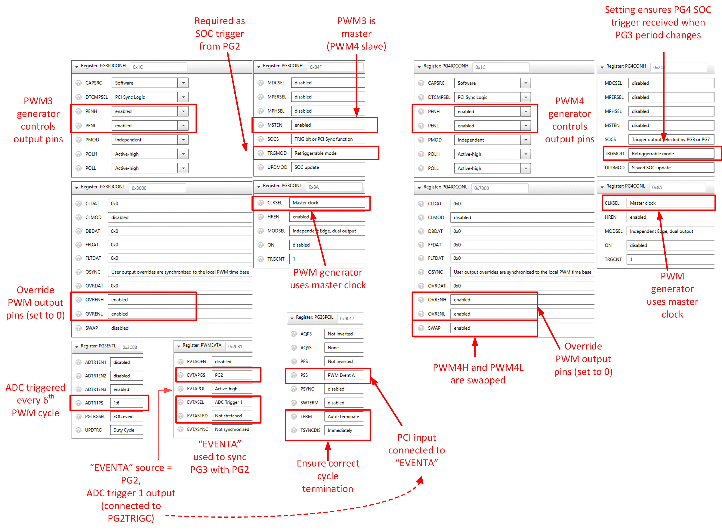
The fields that need to be modified for phase B (related to PWM3 and PWM4) are highlighted below.
In this section we describe how to measure the open loop gain and phase of the plant, and show some results that we took from the LLC board. We then discuss the compensator used to regulate the output voltage and show some open loop gain measurements of the closed loop system at different operating points.
It can be useful to measure the open loop frequency response of the plant, to allow the compensator to be designed appropriately. In this section we describe a way to do this on this LLC demo board.
First please read section 1.4 of [MA330048]. This describes how to measure the loop-gain of the plant using the dsPIC33CK256MP506 Digital Power Plug-In Module (DP-PIM) and a vector network analyzer such as the Bode 100 from Omnicron.
In this instance, we made some small modifications to the procedure described in the DP-PIM user's guide.
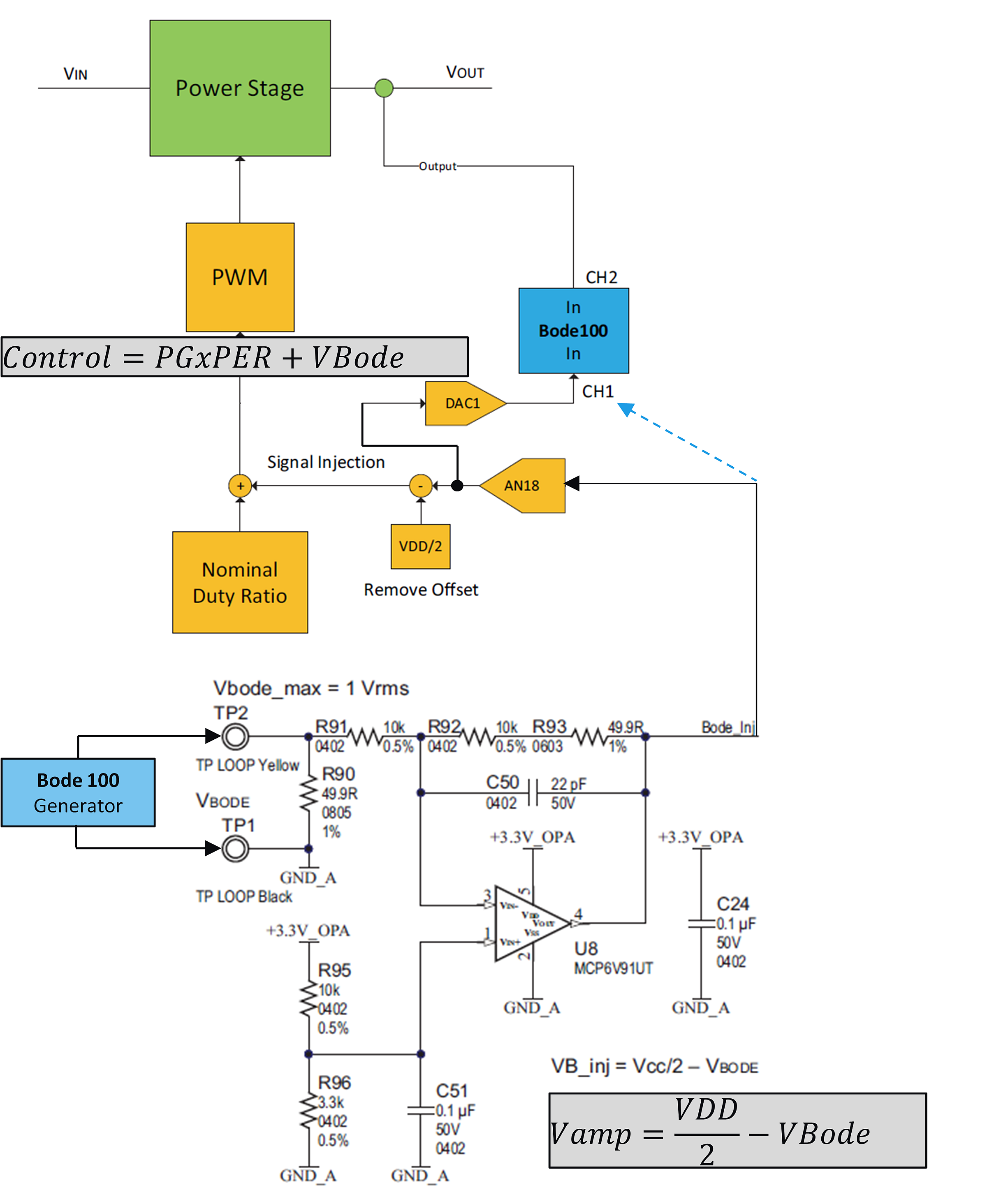
In the diagram above, circuitry inside the dsPIC is designated by an orange colour. Blue blocks are measurement circuitry (from the Bode 100 in our case). The plant is shown in green. The operational amplifier circuitry is on the DP-PIM. The Bode 100 generator output (which creates a small AC sinusoid that is swept over frequency as part of the open loop frequency response measurement) is connected across TP1 and TP2 of the DP-PIM. This signal then passes through an operational amplifier circuit on the DP-PIM. The purpose of the operational amplifier circuit is to add an offset of 1.65V to the AC signal, as the ADC on the dsPIC can only digitize positive voltages and the output of the Bode 100 is AC.
This AC signal with a 1.65V DC offset is then digitized by the ADC on pin AN18 of the dsPIC. The ADC code equivalent to the 1.65V DC offset is subtracted in the firmware, and the result (which is a digitized AC signal) is added to the control input. Thus the control input is "disturbed" by this digitized AC sinusoid. For an LLC, the control input modulates the switching frequency. So as the control input moves up and down, so will the switching frequency.
The plant frequency response measurement includes the digital modulator and so is calculated as "control to output".

This is a measure of how much Vout varies in gain and phase as the control input is disturbed. Each measurement point corresponds to a frequency, this is the frequency of the AC signal disturbing the control input. The frequency of the AC disturbance is swept from almost DC to (usually) the ADC sampling frequency / 2.
This means that channel 1 of the Bode 100 should be connected as close as possible to where the control input is disturbed. Channel 2 of the Bode 100 should be connected to the output of the converter.
Channel 1 could be connected directly to the AN18 pin. In this case, the plant gain measurement would be accurate, but the measurement of the phase response would not be accurate at higher frequencies because of the ADC sampling delay (as the disturbance and Vout are sampled at a frequency of Fsw/6). Hence, we take the ADC measurement on AN18 and convert it back to the analog domain by loading the digital value into a DAC on the dsPIC. This leads to a more accurate phase measurements at higher frequencies.
Setup the firmware so that the converter is running in open loop mode, you can even remove the compensator from the code if you wish.
Configure the firmware to run in interleaved mode.
To setup the dsPIC to measure the disturbance on the AN18 pin, MCC can be used as shown below. For our measurement, we used the shared ADC core to measure both the output voltage and the disturbance.

We use the shared ADC core to measure both the disturbance and Vout. Firstly, we measure Vout with the shared ADC core. Then the shared ADC core conversion channel is changed manually to measure the voltage on the AN18 pin. For example, the firmware below can be added to the function ADCAN0Interrupt() in the file driver/drv_adc.c. It can be added just after the two secondary phase currents are sampled with the ADC.

The measurement of the voltage on AN18 (with the 1.65V DC bias removed) is stored in pwr_ctrl_adc_data.drv_adc_val_AN18. Note that since the DC bias has been removed, this result can be negative or positive. This is correct as we want to control input to move in both directions.
We need to apply this disturbance to the control input. In the function Drv_PwrCtrl_ILLC_ILPHVoltageLoop(), we added the following code for this purpose.
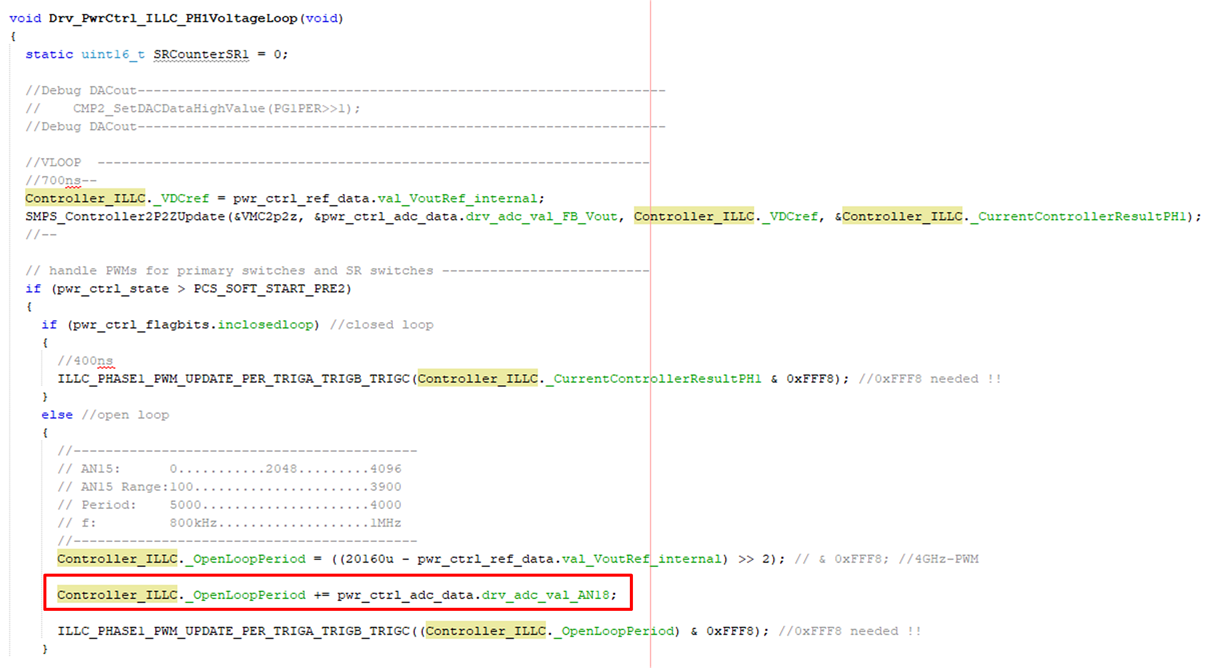
In the line highlighted above, the disturbance is added to the control input. Note that the disturbance at this point has been digitized and the DC bias has been removed, so this line adds the (digitized) small signal AC disturbance to the control input. It can cause the control input to both increase or decrease.
In the final line of the code snippet above, the control input is converted to a period for the PWM peripherals, as the switching period is modulated for the LLC topology.
Finally, we take the ADC measurement of the voltage on AN18 (that is, the disturbance input from bode measurement instrument) and load this digital value into DAC2 (which is connected to pin 17, and also to the test point on the top of the DP-PIM). To this end, this line should be added after the control input is updated. The output of DAC2 is measured with channel 1 of the Bode 100.

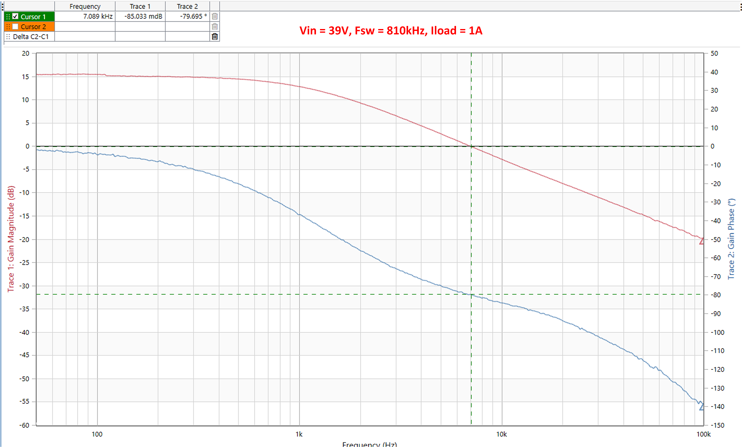
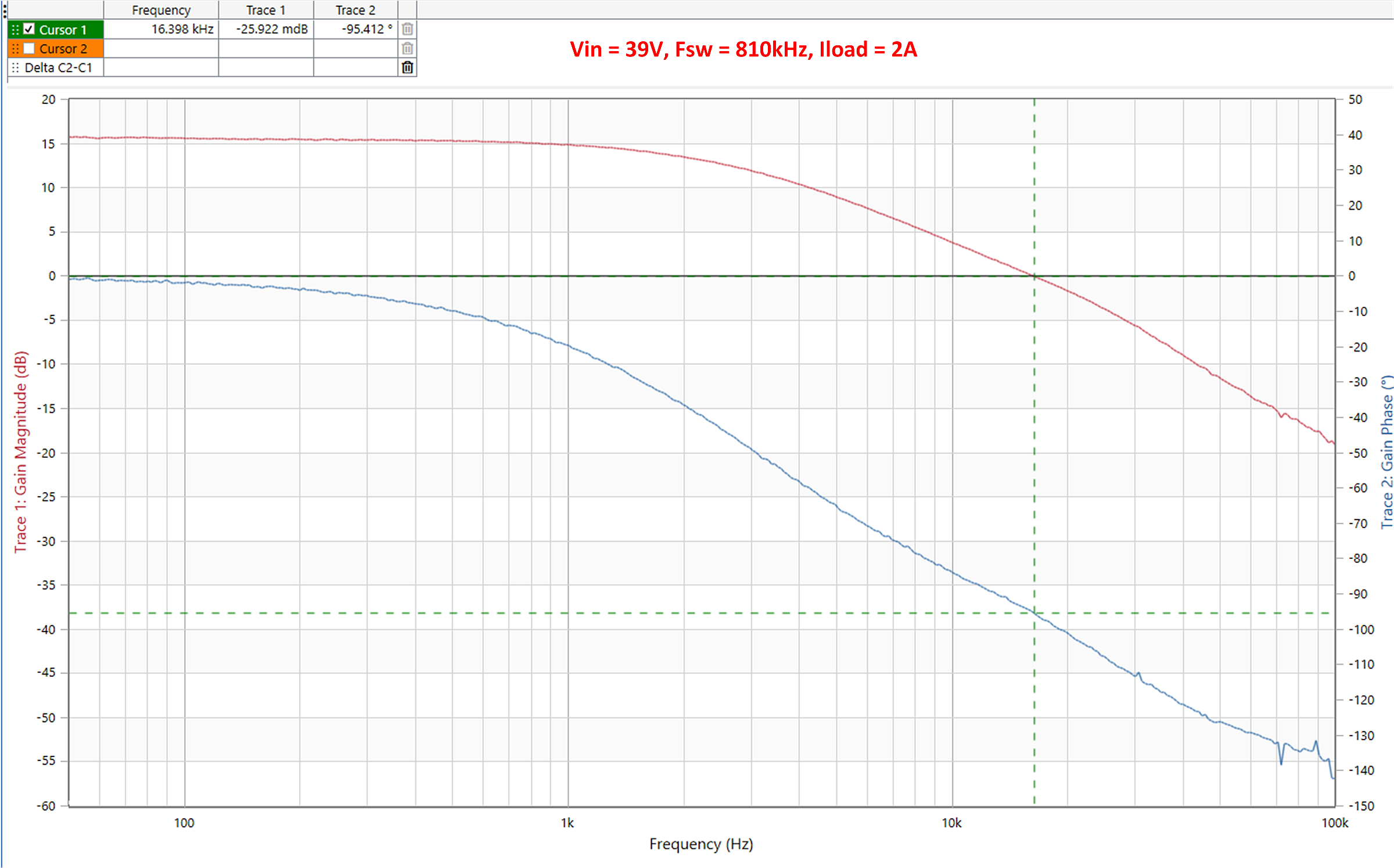
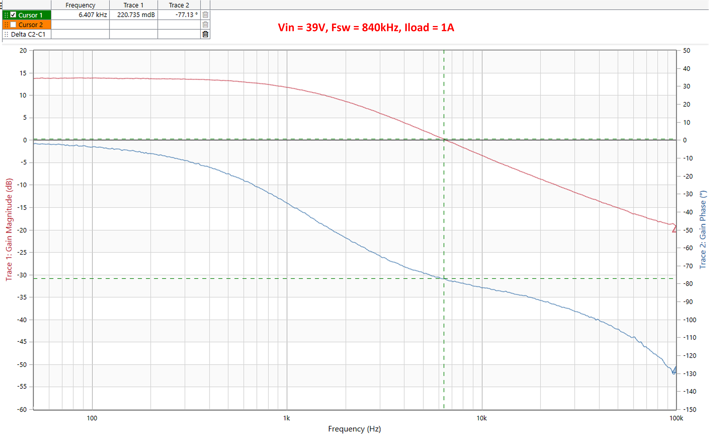
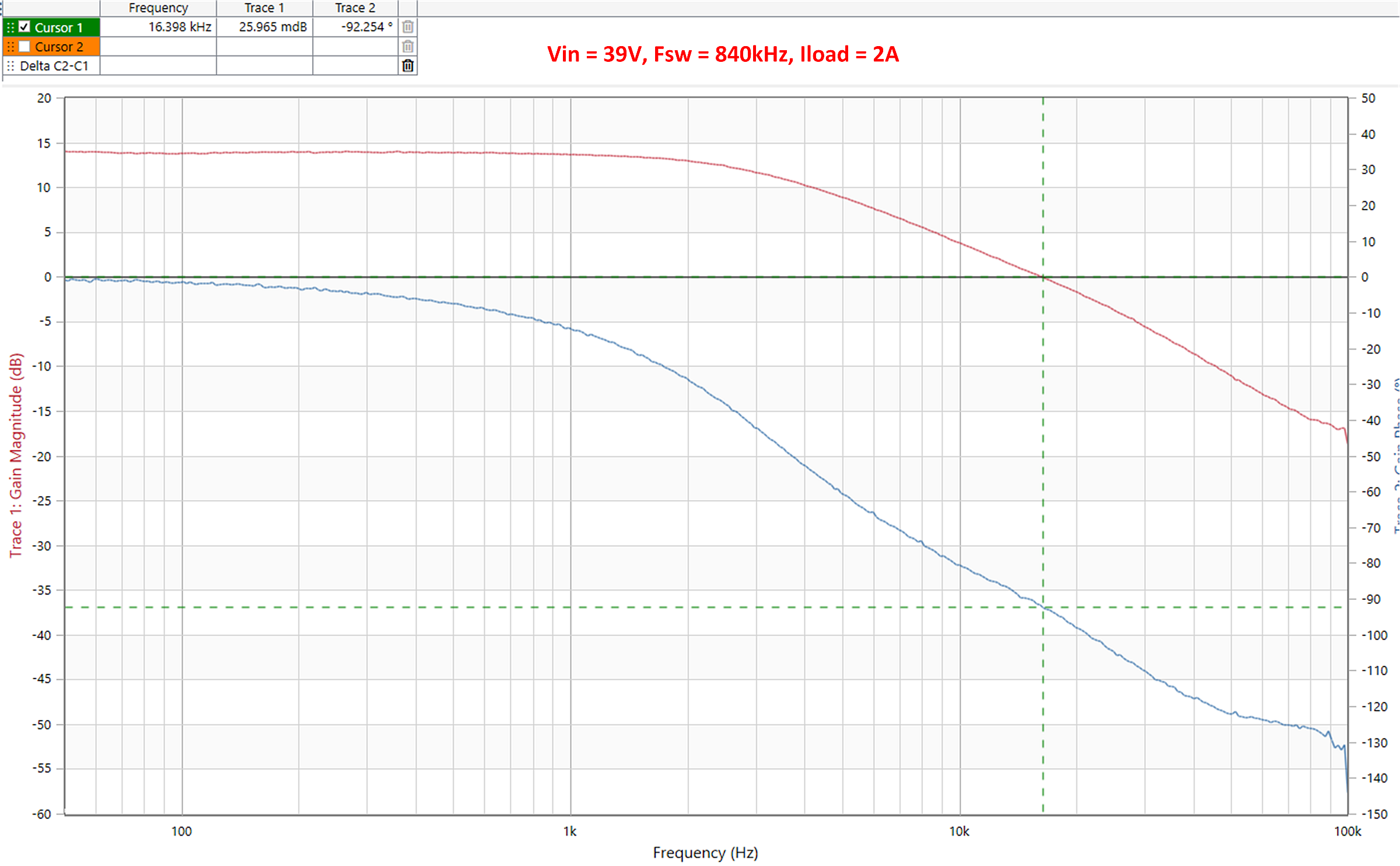
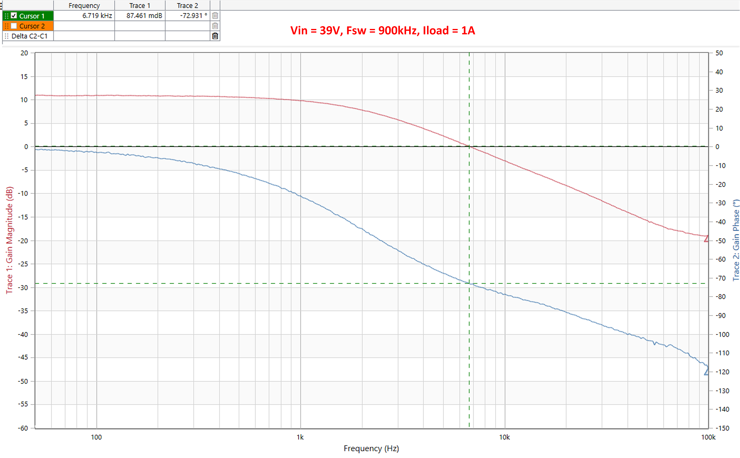
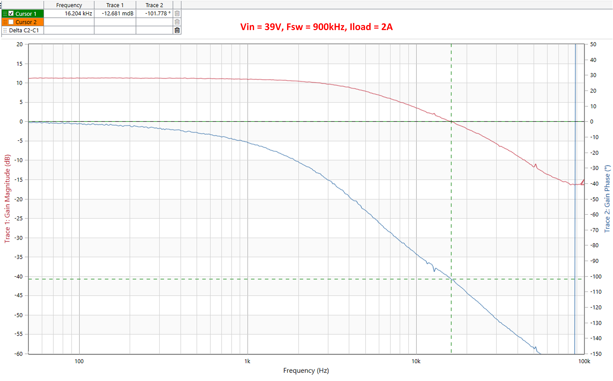
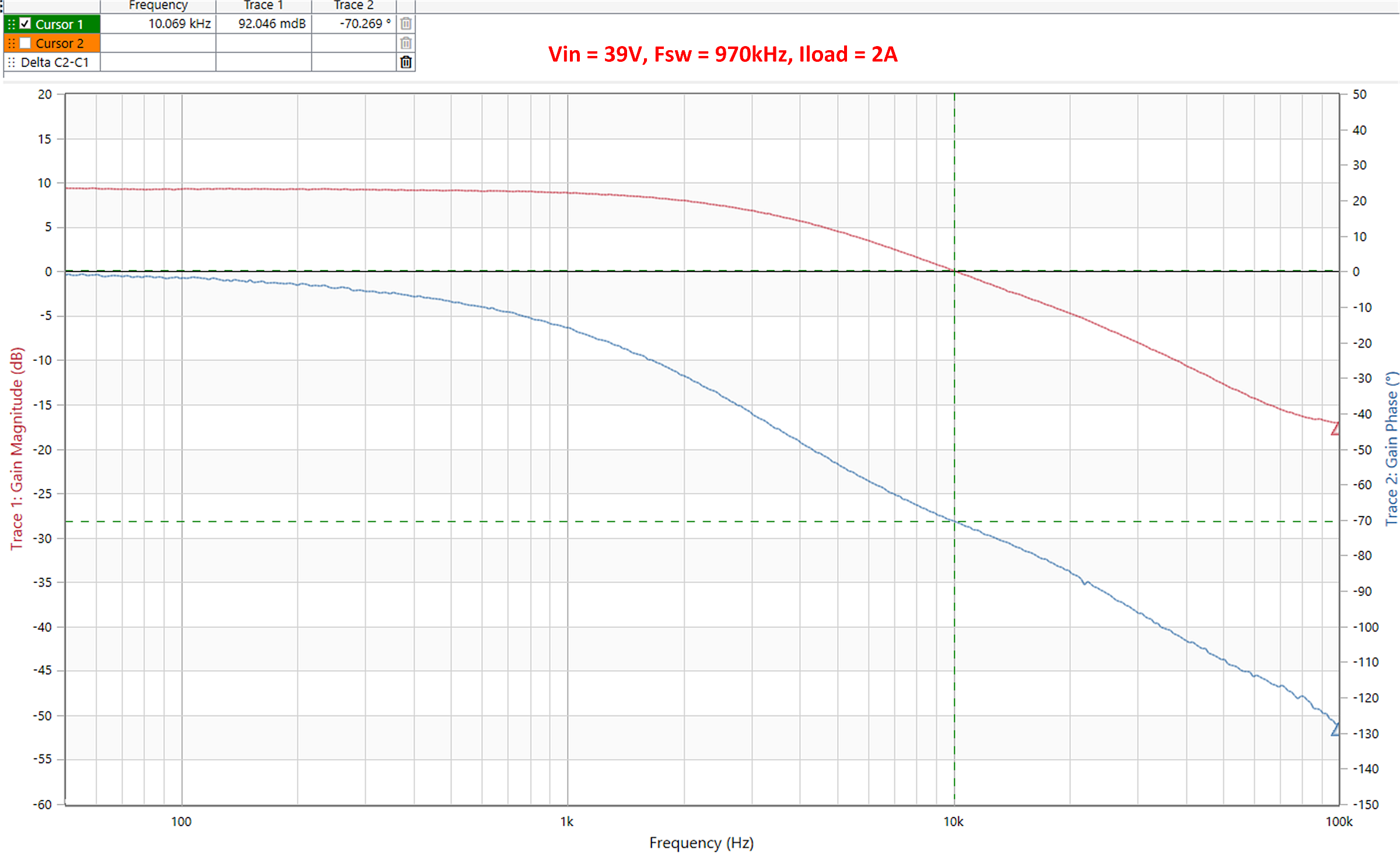
Here we show the results at multiple operating points, running in interleaved mode. We use the potentiometer to change the switching frequency in open loop mode for these measurements. A resistive load is used.
Note that the gain and phase response moves quite a bit depending on the switching frequency and load. For an LLC converter, the plant is "dynamic" and thus pole and zero positions will move depending on the operating conditions.
For example, at 1A load, the SRs on the secondary side are disabled, this adds dynamic resistance in the conduction path and changes the measured plant frequency response. At 2A load, the SRs are enabled, meaning less dynamic resistance. This can be seen in the plots below.
Thus it is important to run these measurement at many different operating points to ensure that the compensator is designed for worst case conditions.

Since the plant frequency response is single pole system, it is sufficient to use voltage mode control to compensate for the plant, using a 2P2Z compensator.
As this is a frequency controlled converter, the control algorithm controls the PWM switching frequency to regulate the output voltage.

Digital Compensator Design Tool, abbreviated to DCDT, was used to design the 2P2Z compensator.
To download and install DCDT, please follow the instructions at the link above.
To open DCDT from MPLABx, click "Tools -> Embedded -> Digital Compensator Design Tool".
On the pop-up window that appears, click "Open", which will open the "VMC" DCDT project associated with the LLC MPLABx project.
On the next window that appears (shown below) click on the compensator block.
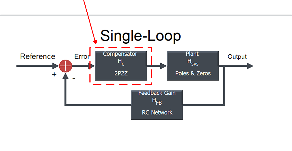
The compensator settings in DCDT are shown below.
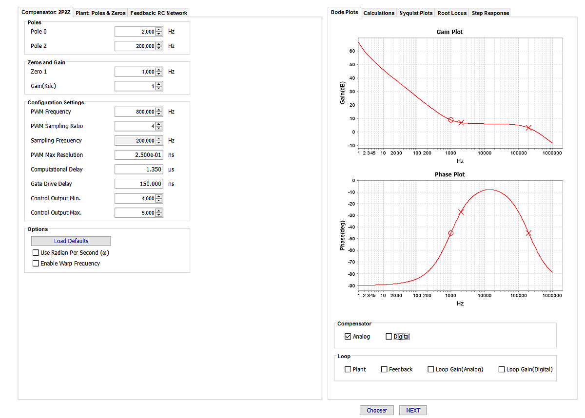
As can be seen above, for our 2P2Z compensator (which has 2 poles and 1 zero), we placed
Note that for this demo firmware, we tuned the compensator empirically. For a 2P2Z compensator, typically the second pole is placed at high frequency (usually half of the ADC sampling frequency) to filter the effects of high frequency ripple and noise on the loop. The zero is typically placed at a low frequency, perhaps somewhere between 200Hz and 500Hz to begin with. The purpose of this zero is to ensure that you have enough phase at the cross-over frequency. The pole at origin is set to get as much DC gain as possible.
In this example, we started with a conservative coefficient set and moved the zero and pole at origin until our measured frequency response was deemed satisfactory.
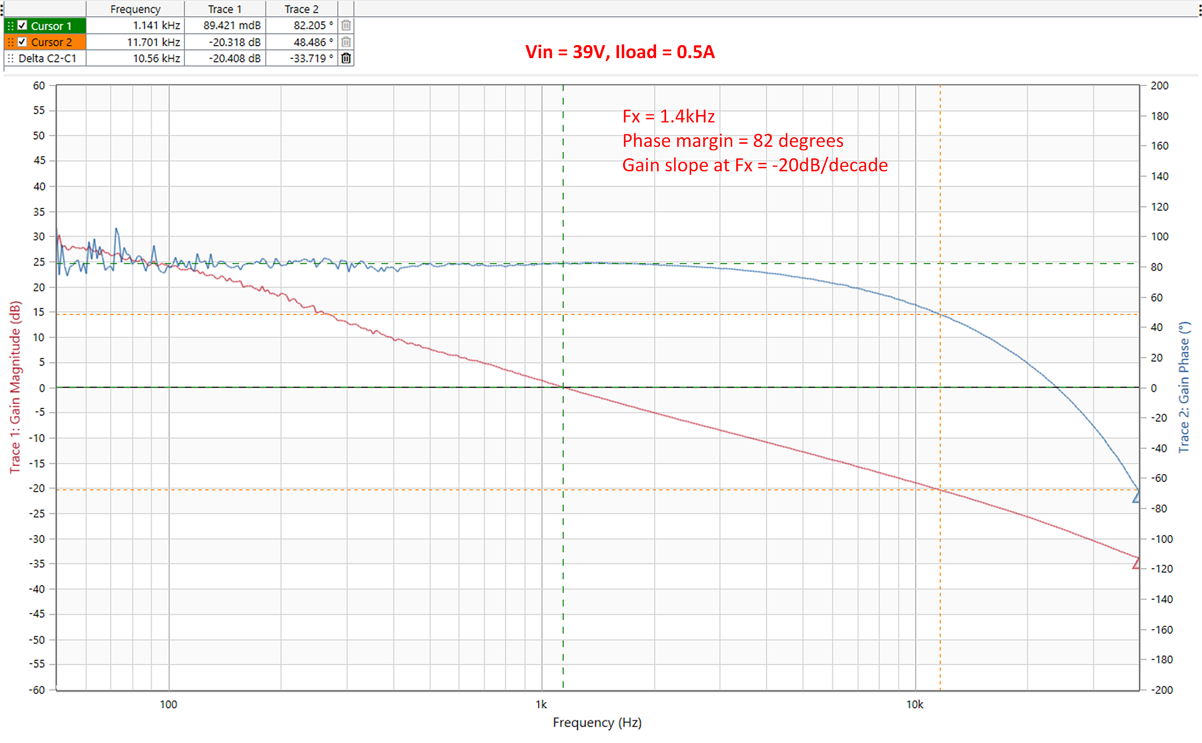
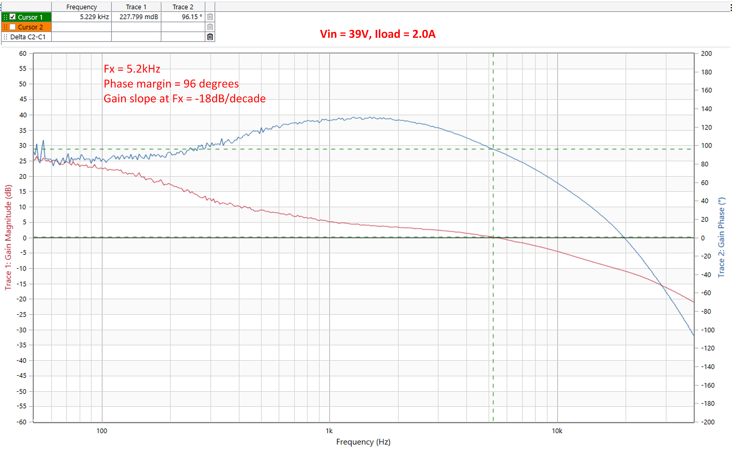
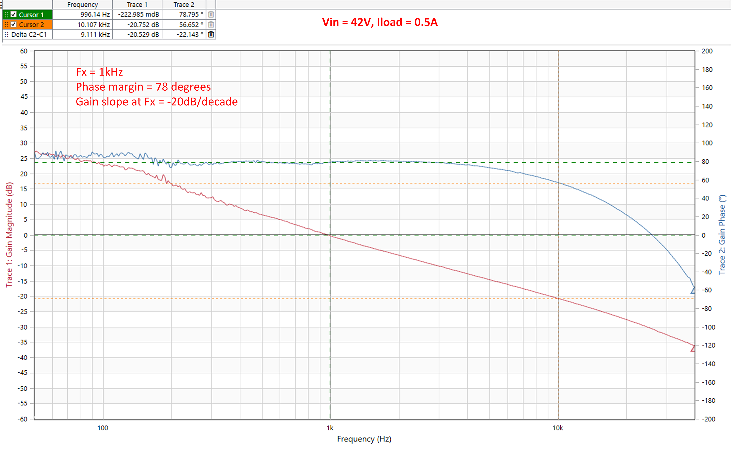
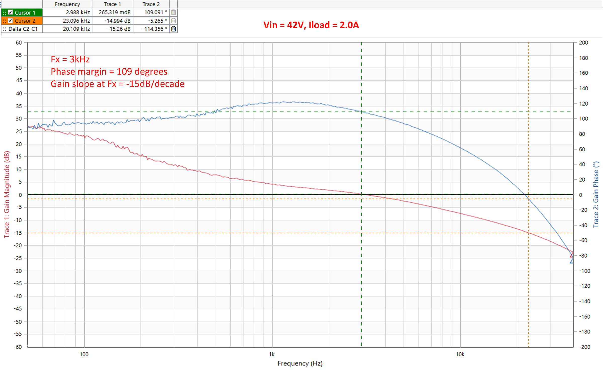
In this section we shown the open loop gain and phase response. To clarify, these are the "open loop" measurements of the closed loop system - so the measurements include the plant, the voltage feedback network and the 2P2Z compensator.
For these measurements, the Bode 100 output was connected across the 20R resistor R120, using the test points TP120 and TP121. This resistor was placed between the output terminal of the converter and the resistor divider used for output voltage sensing by the dsPIC.
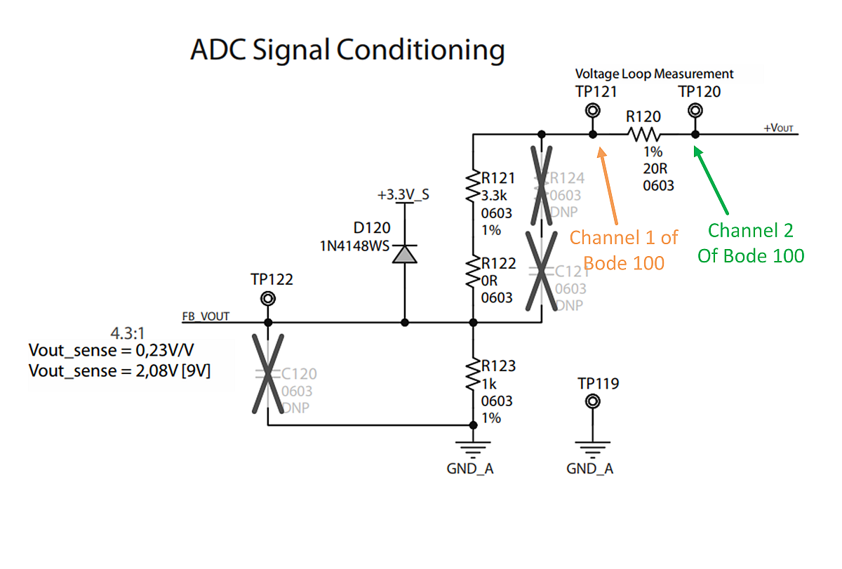
Channel 2 of the Bode 100 was connected to TP120, and Channel 1 was connected to TP121. See below for measurements taken across different load settings and input voltage settings.
Note that the crossover frequency, phase margin and slope of gain at the crossover frequency changes depending on the load and input voltage. At 0.5A load, the SRs (and thus the current balancing scheme) are disabled, which slows down the loop response versus the measurements taken at 2.0A load.
When two or more identical half-bridge LLC converters are interleaved, any differences in their tank circuits will lead to unequal sharing of the load current between individual phases. Unequal load sharing is a major problem in interleaving resonant converters as it decreases thermal stability and can lead to high-circulating currents and even converter failure.
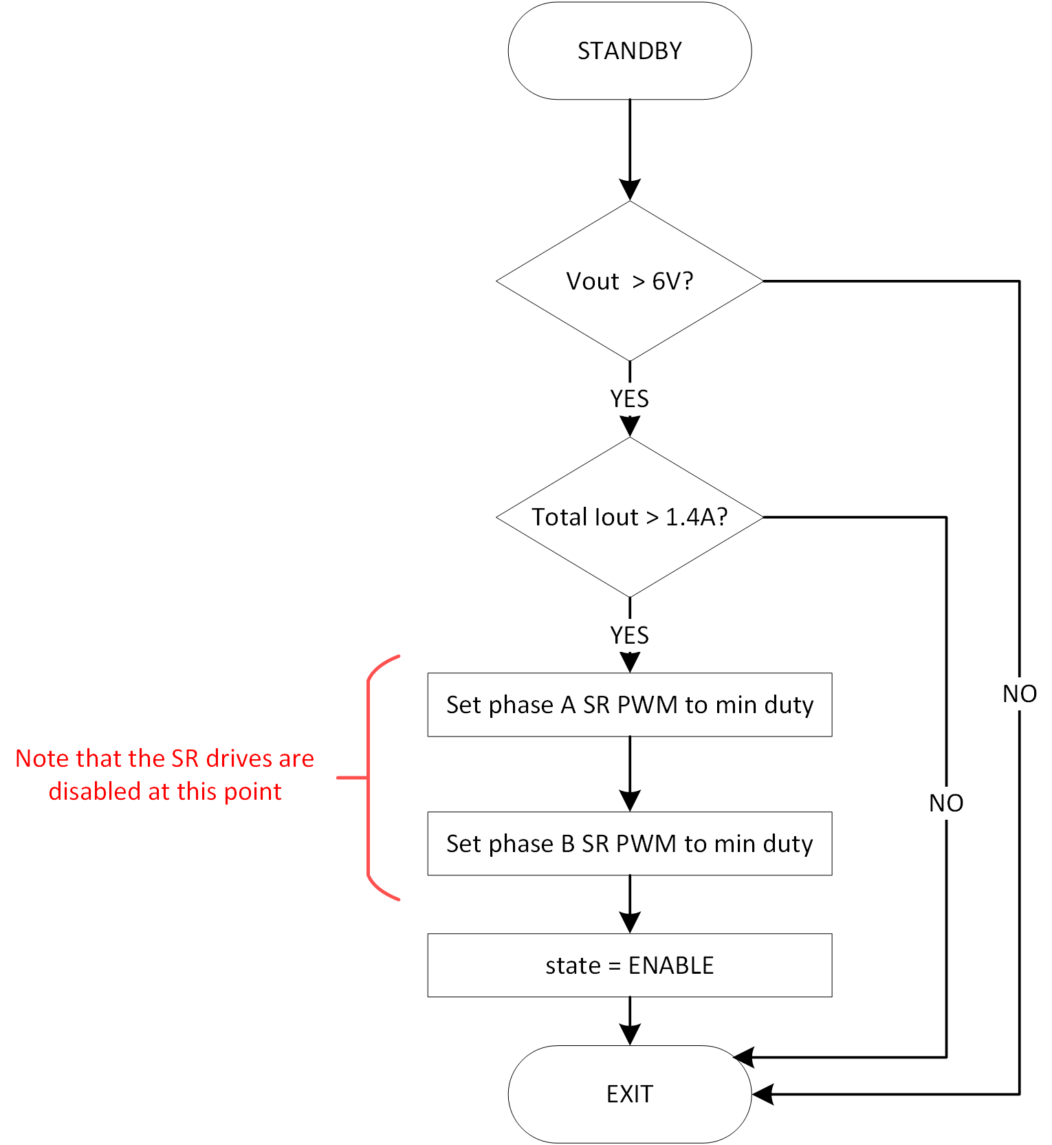
A innovative current balancing scheme has been implemented on the demo firmware accompanying this board. The goal is that both phases share the load current equally. This scheme is only run if the total load current is above 1.4A (see the macro IOUT_SRONIL_in the firmware). The code is located in the function_Drv_PwrCtrl_ILLC_ILPHVoltageLoop(), which is in the file power_controller/drv_pwrctrl_ILLC_SRandControl.c. This function is called from the ADCAN0 interrupt, which is located in the file driver/drv_adc.c.
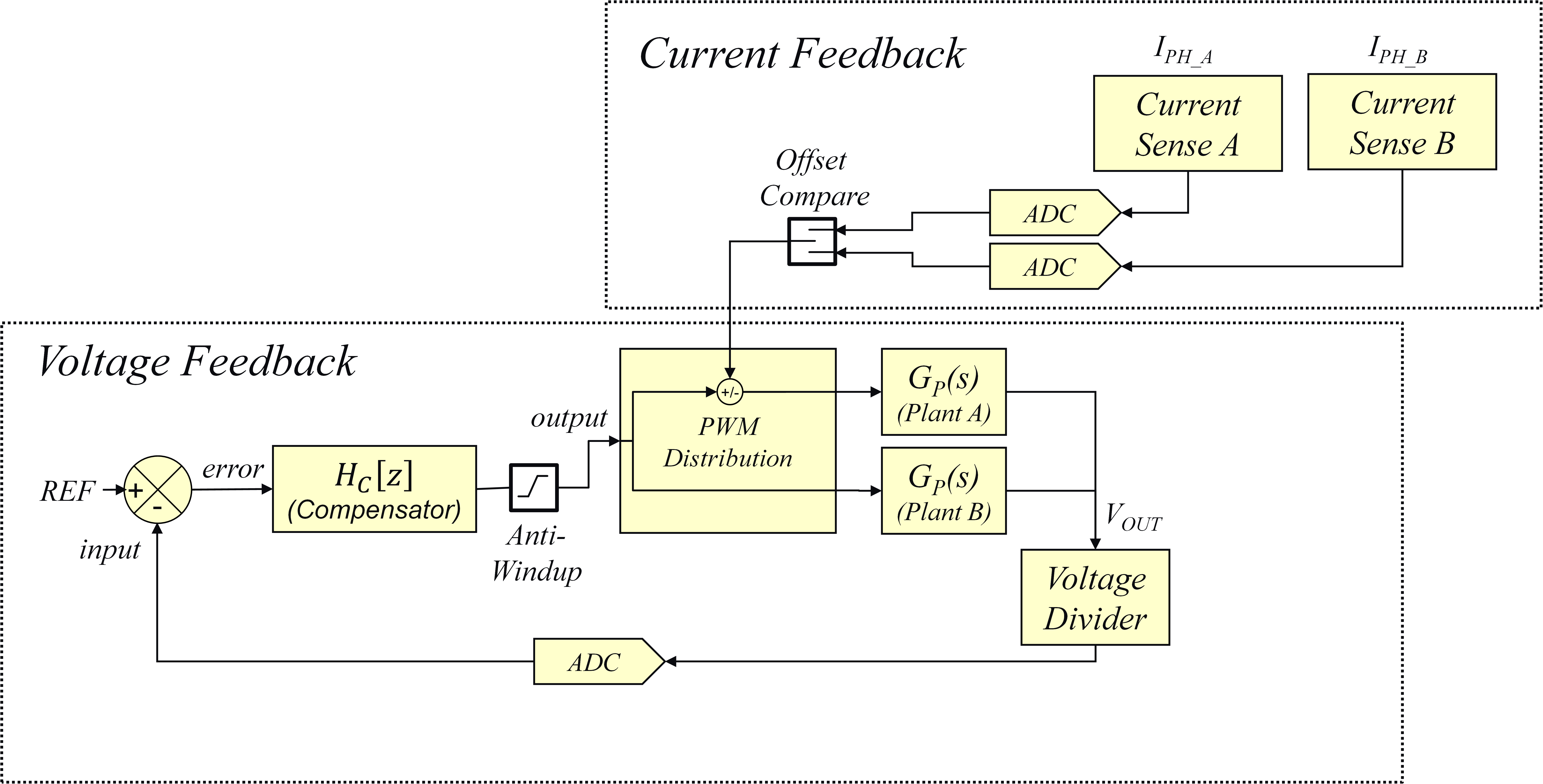
The scheme works by changing the duty cycle of the SR drive signals on one phase until both phase currents are approximately the same, while keeping the duty cycle of the SR drives on the other phase fixed.
When the scheme is launched, the (filtered) currents of both phases are compared. The phase with the smaller current runs at a fixed (just under 50%) duty cycle, while the duty cycle of the SRs on the phase with the larger current is varied between a min value (100ns) and a max value (just under 50%) until the two currents are as close as possible.
Decreasing the duty cycle of the SR drives on one phase increases the dynamic resistance presented to the secondary current flowing through this phase. This results in less current flowing through the phase and more through the other phase. The total output current remains the same.
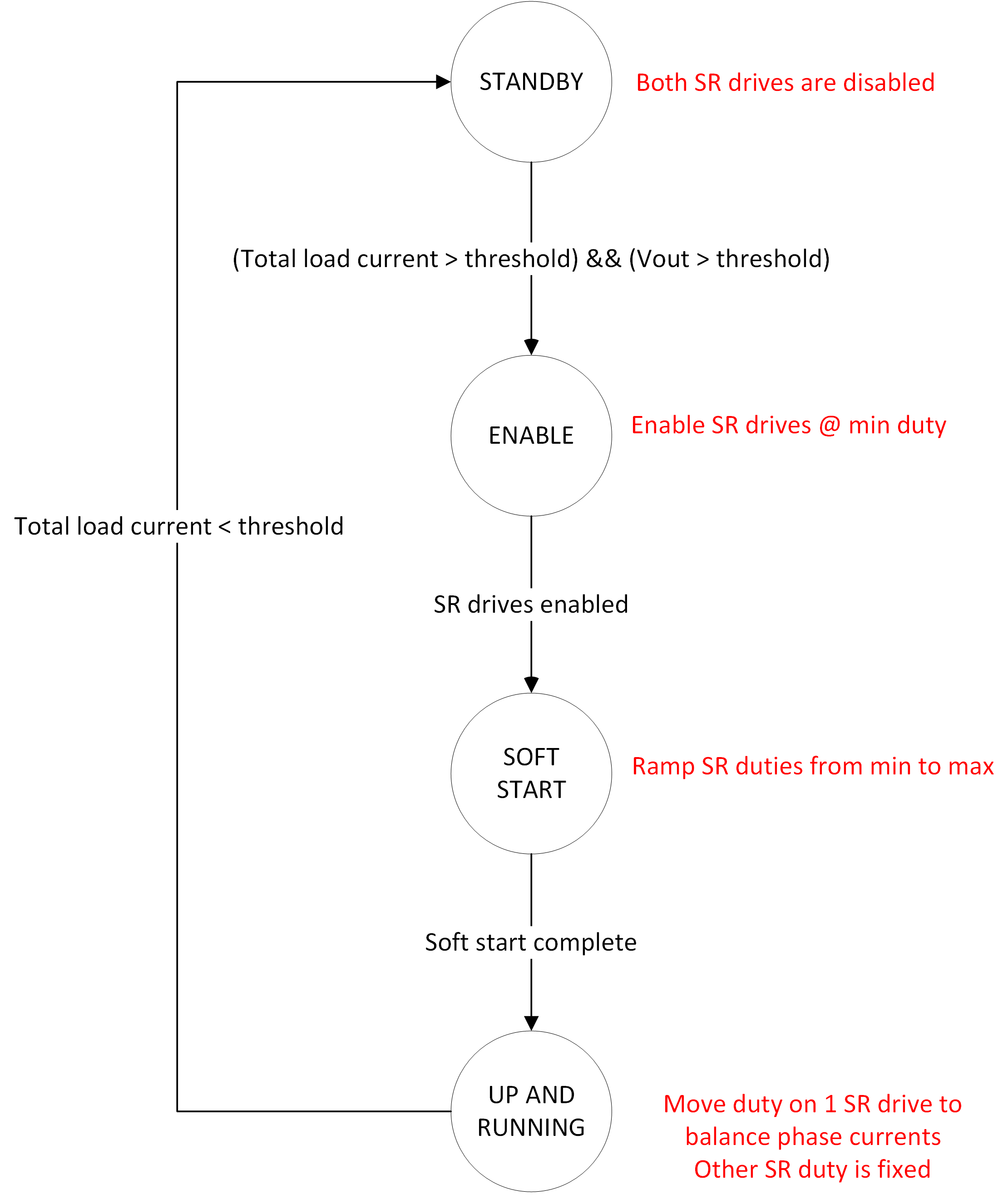
The state machine that runs the current balancing algorithm is illustrated above. It is run in the ADCAN0 interrupt, which is executed every 6th PWM period.
Both SRs are disabled, so any conduction is through the body diodes of the SRs. We stay in this state until the output voltage is above 6V (see macro VOUT_SR_ACTIVE) and the total output current is above 1.4A (see macro IOUT_SRONIL). If both of these conditions are satisfied we go to the enable state.
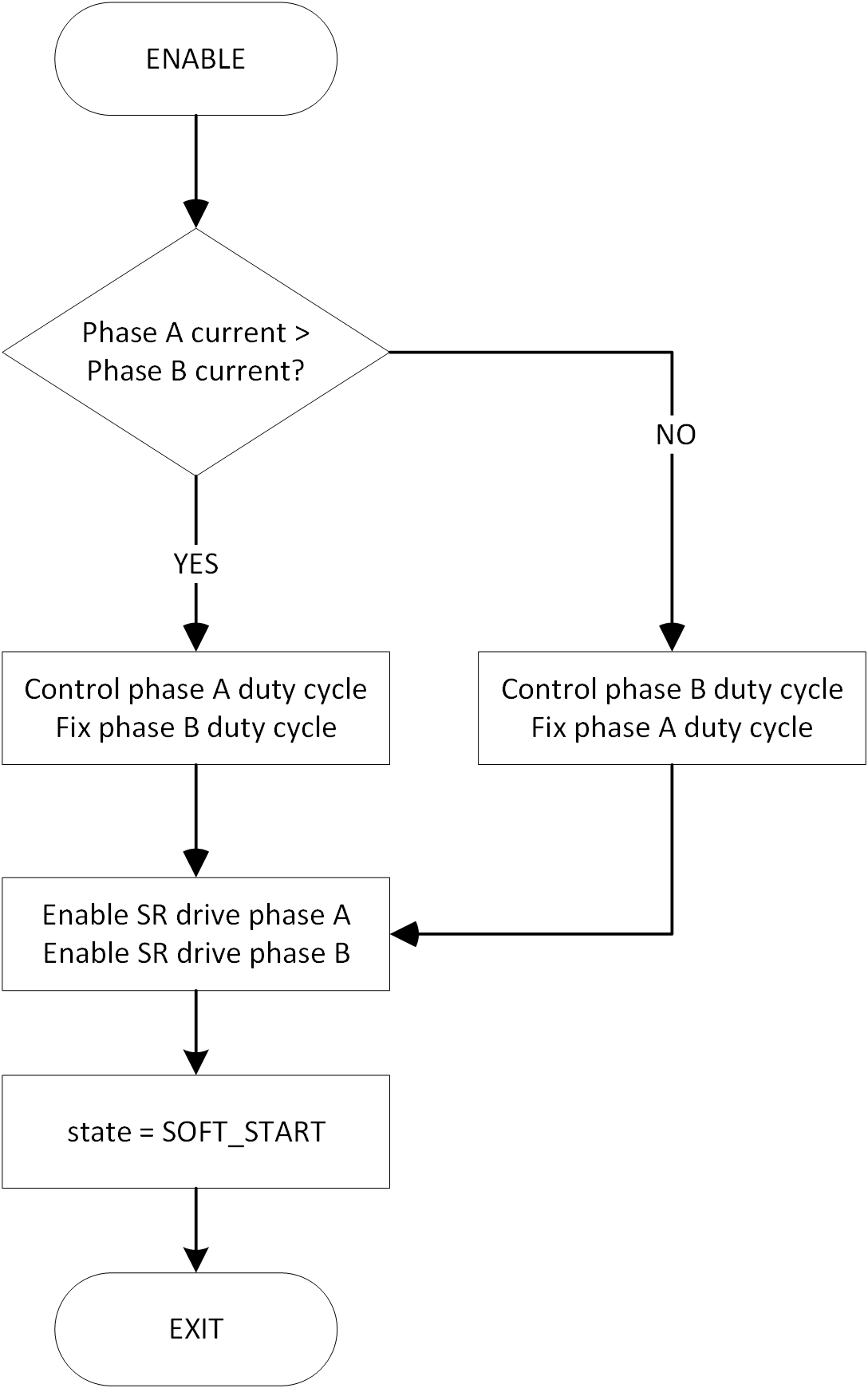
Both SRs are still disabled. The two phase currents are compared. In our current balancing algorithm, the phase with the smaller current has a fixed SR duty cycle, and the SR duty of the other phase is varied to get the currents in balance. So the decision on which phase to fix and which to vary is made once at this point, and remains in force while the algorithm is active.
Note that the phase current measurements used for the comparison are filtered to reduce the effect of noise on the decision.
After the comparison is made, PWM2 and PWM4 (the PWMs used to drive the SRs for phase A and phase B respectively) are enabled and set at min duty cycle. The PWM setup is actually done in the STANDBY state, but the PWM outputs from the dsPIC are not enabled until the ENABLE state.
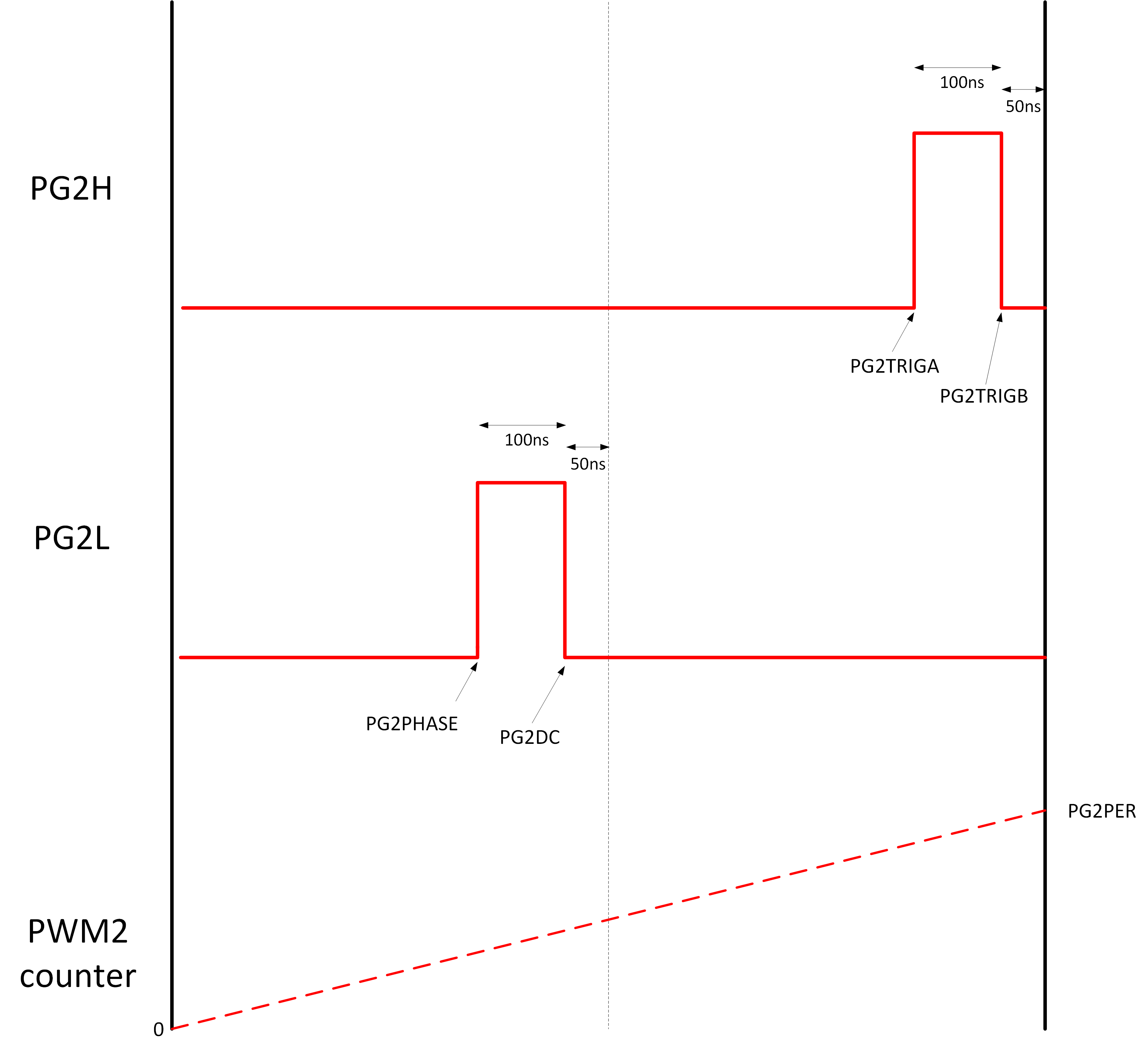
As discussed previously, the PWMs are configured in "Independent, dual output" mode. To recap, PG2 is used to drive the SRs for phase A, and PG4 is used to drive the SRs for phase B.
For phase A, the rising edge of PWM2H is set via the PG2TRIGA register (so the event is triggered when the internal period counter in PG2 reaches PG2TRIGA), and the falling edge set via PG2TRIGB. The rising edge of PWM2L is set by the PG2PHASE register, and the falling edge via the PG2DC register.
For phase B SR drive, PG4 is used, so PG4TRIGA, PG4TRIGB, PG4PHASE and PG4DC are used to set the rising and falling edges on PG4H and PG4L in the same way as for PG2.
In this state, the duty cycles of the SR drives on both PG2 and PG4 are linearly ramped from the min duty (100ns pulse width) to the max duty (PGxPER/2*250ps - 124ns) in steps of 10ns.
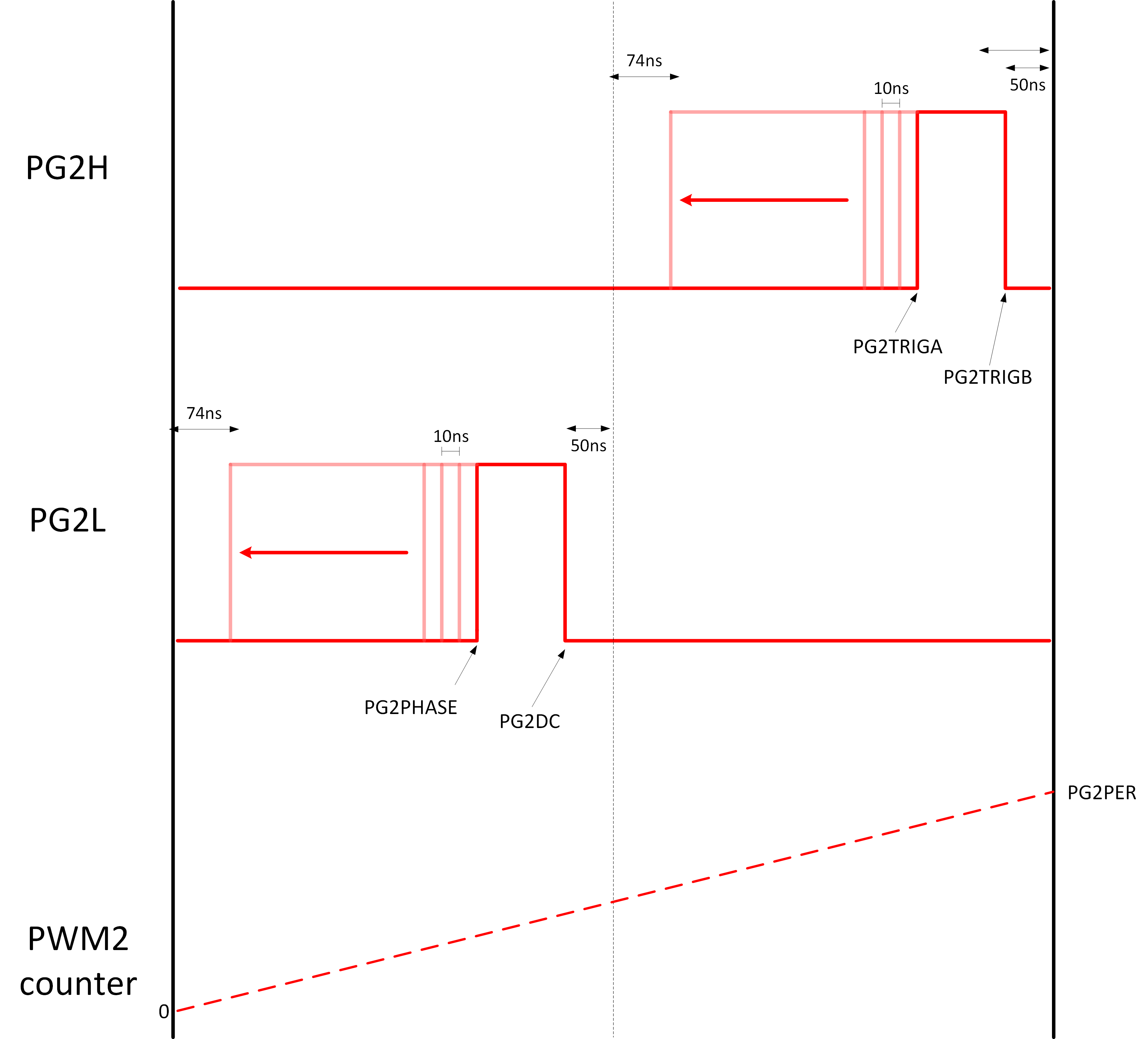
The falling edges of the PWM2 and PWM4 outputs are fixed during the ramping of the duty cycle, and the rising edges are moved. For PG2, PG2TRIGB is fixed at 50ns before the end of period, and PG2DC fixed at 50ns before the end of the half-period. For PG4, PG4TRIGB is fixed at 50ns before the end of period, and PG4DC fixed at 50ns before the half-period.
During the soft-start ramp, PG2TRIGA, PG2PHASE, PG4TRIGA and PG4PHASE are decreased by steps equivalent to 10ns so that the duty cycle increases by 10ns each time.
The ramp is stopped when the rising edge of PG2PHASE is 74ns from the start of the period. Thus at the end of the ramp, all SR drive signals are running at just under 50% duty cycle (precisely, the on-time is [PG2PER/2*250ps] - 124ns).
At the end of the ramp, we change to the UP AND RUNNING state.
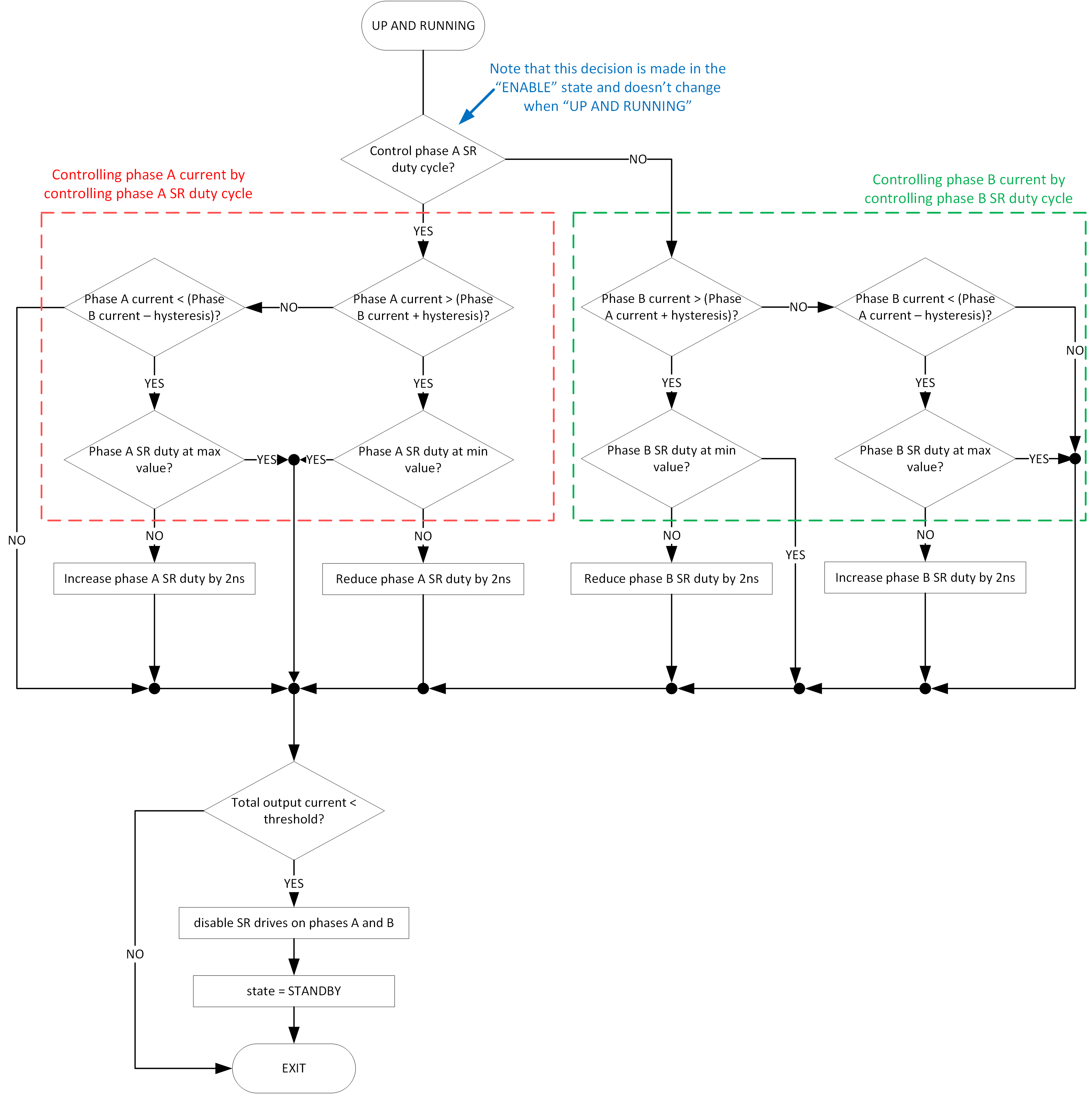
In this state, one of the SR drives of either phase A or phase B runs at a fixed duty cycle, and the other is moved. The decision on which phase to fix and which to vary is made in the ENABLE state and doesn't change thereafter.
If the output current through the phase being controlled is greater than the current through the other (fixed duty) phase, we decrease the duty cycle of the SR drives by 2ns. If the current is smaller, we increase the duty cycle on the SR drives by 2ns. The on-time of the SR drives is clamped at a max value of [PGxPER/2*250ps - 124ns], and at a min value of 100ns.
If the total output current drops below 1.0A (see macro IOUT_SROFFIL), all SR drives are disabled, and we go back to the STANDBY state.
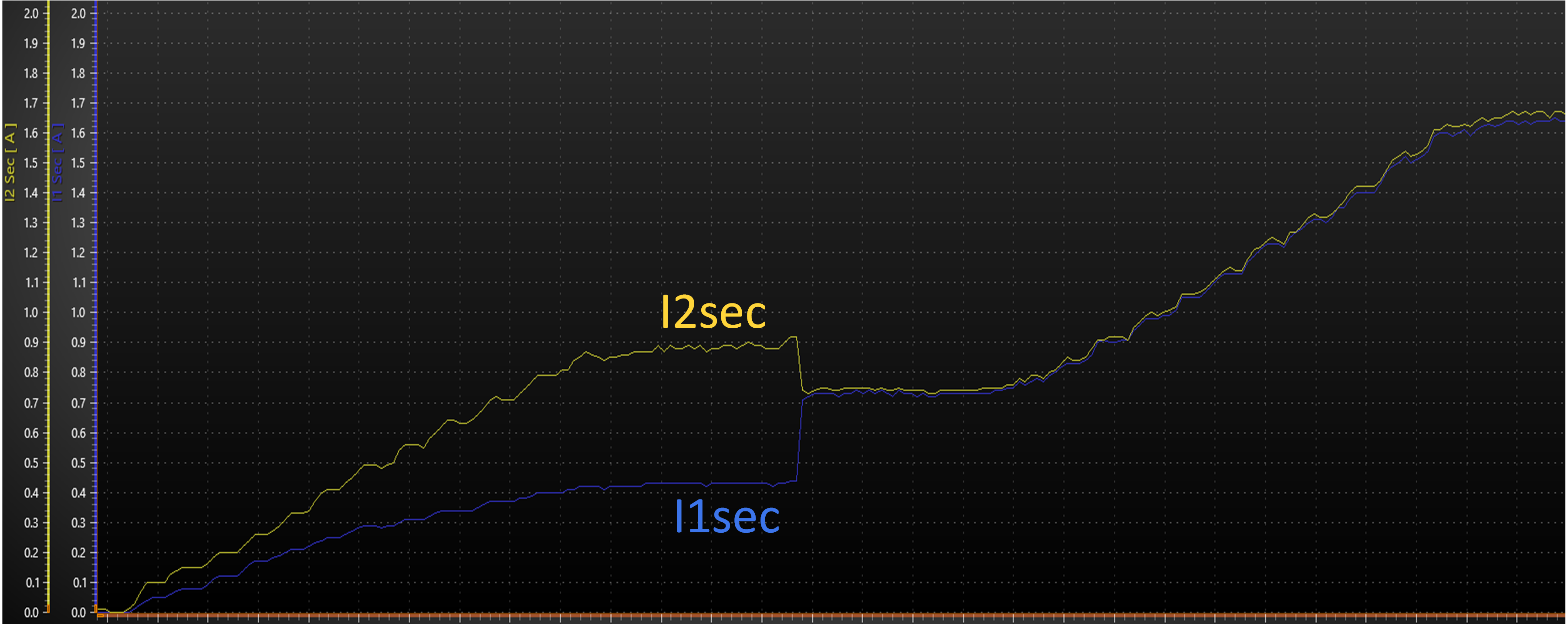
See results below. The two phase currents are out of balance until the total output current reaches 1.4A, at which point the current balancing algorithm kicks in, and the current is shared equally between the phases.
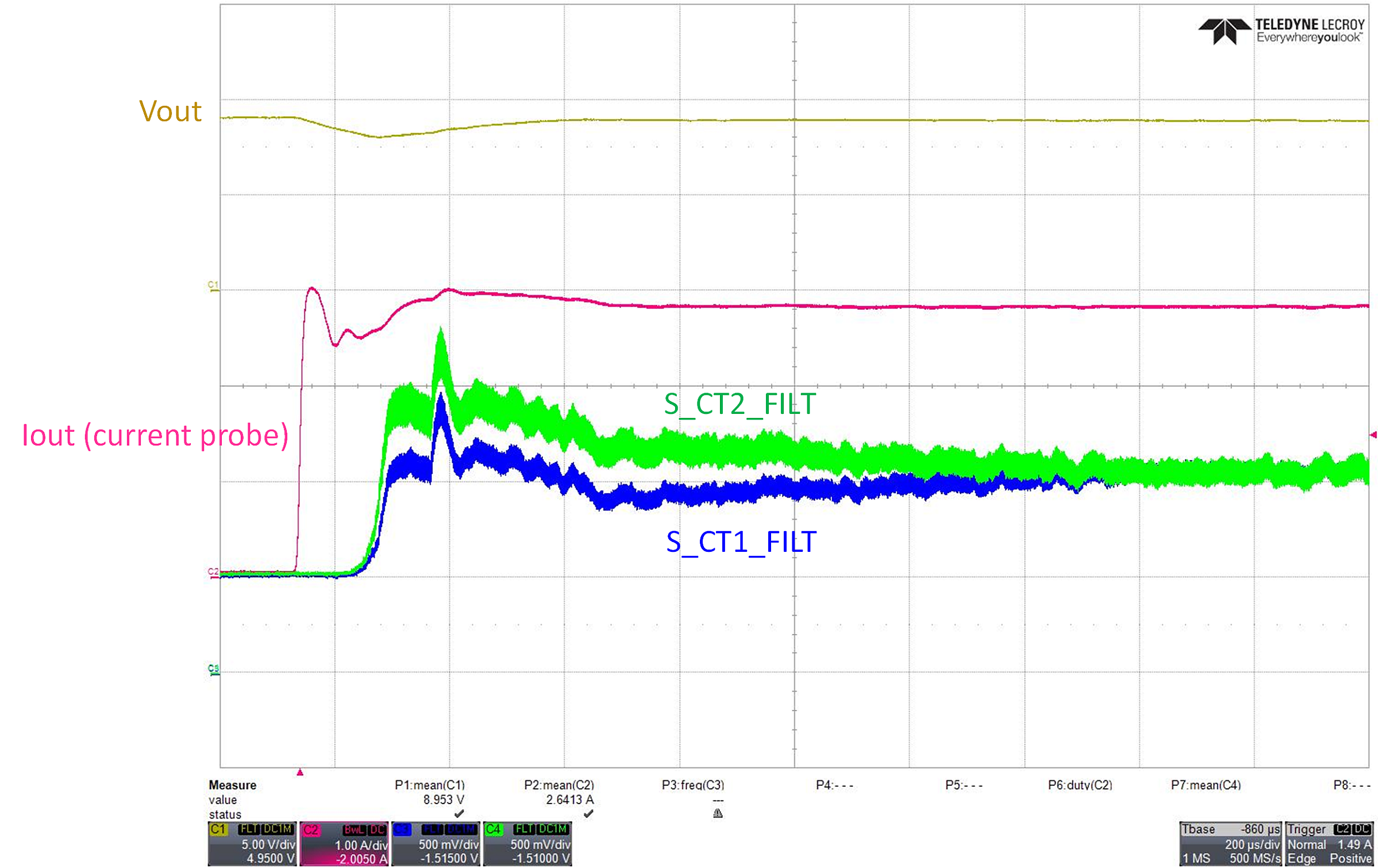
Below we show how it works with a load step from 0 to 3A. The time-base is 200us/div, so you can see that the currents are in balance within 1.5ms.
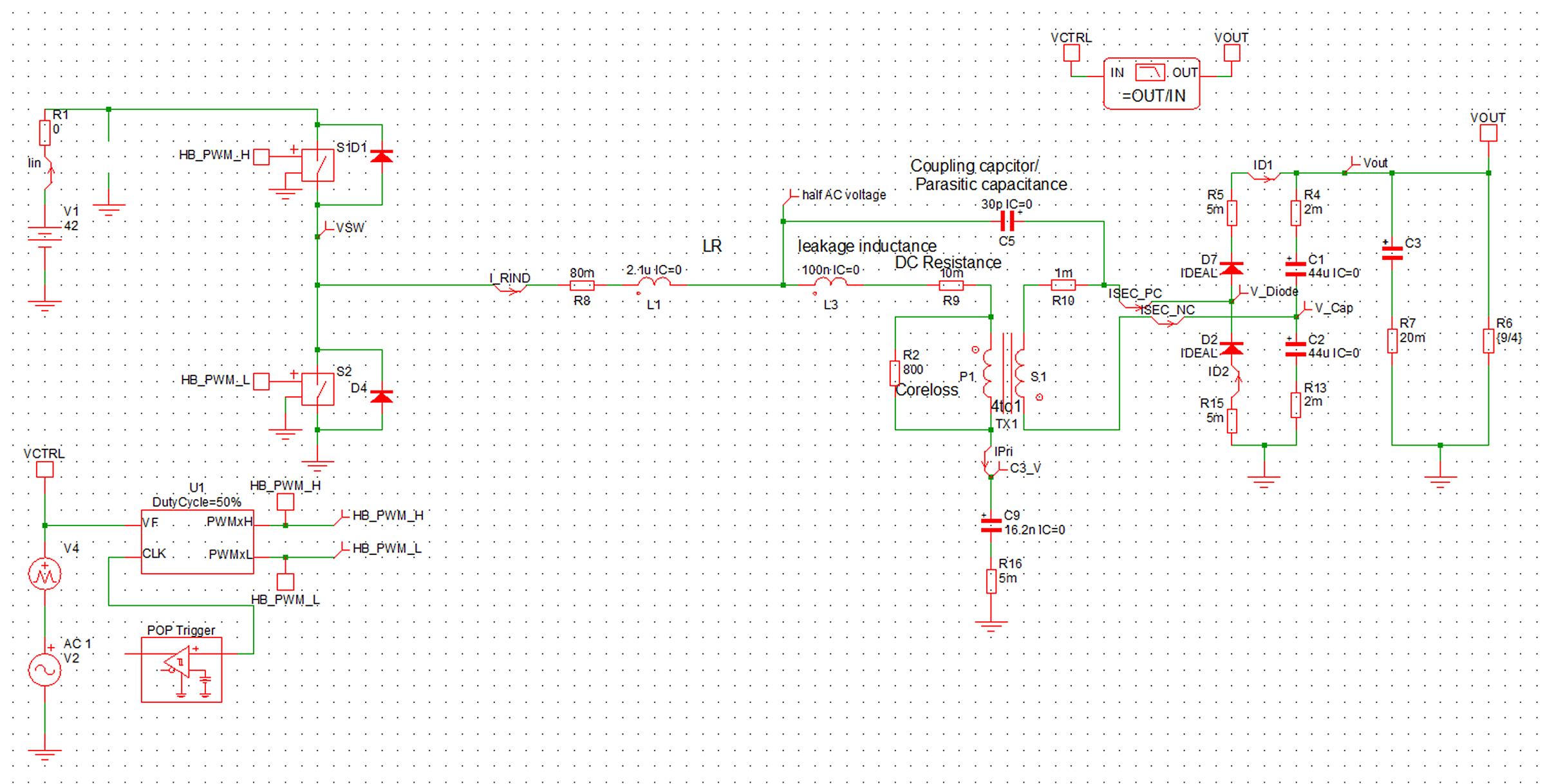
Mindi™ is the Microchip-branded demo version of Simplis/SiMetrix. It supports the common features of the Simplis standard license but limits the number of circuit nodes.
We have included a model of the LLC converter in this deployment for educational purposes. See "mindi" folder.
© 2021, Microchip Technology Inc.