 |
Digital Power Starter Kit 3 Firmware
dsPIC33C Buck Converter Voltage Mode Control Example
|


|
|
Digital Power Starter Kit 3 Firmware
dsPIC33C Buck Converter Voltage Mode Control Example
|
|

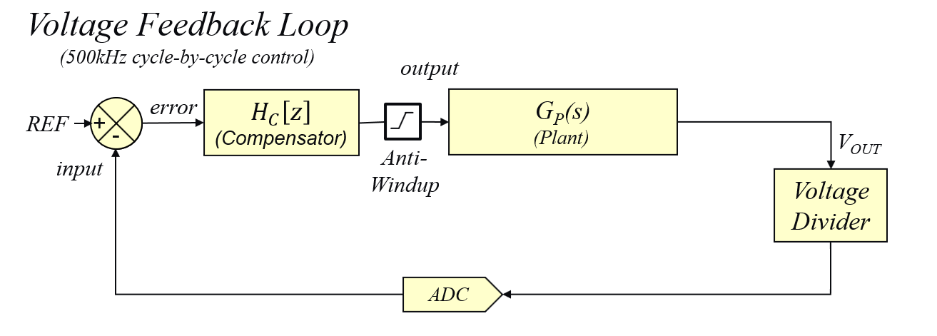
This firmware demonstrates the implementation of a simple, single loop voltage mode controller used to regulate the constant output voltage of the on-board step-down converter of the Digital Power Starter Kit 3 (DPSK3). The implementation of the Voltage Feedback Loop requires one Analog-to-Digital Converter (ADC) input oversampling the output voltage of the converter and two PWM outputs (PWM high and PWM low) to drive the power converter half-bridge switch node in synchronous mode.
[back]
Figure 1 shows the block diagram of the buck converter voltage mode controller, where the ADC input is used to sample the most recent level of the output voltage feedback signal. Once converted, the value is then compared against the internal reference value and the inverse of the deviation between reference and feedback (= error) is pushed through the discrete compensation filter.
In the Anti-Windup block, the output of the compensation filter is checked against user-specified minimum and maximum thresholds. Should any of these thresholds be exceeded, the controller output will be overwritten with the respective threshold value before being written directly to the PWM duty cycle register of the PWM logic.
[back]
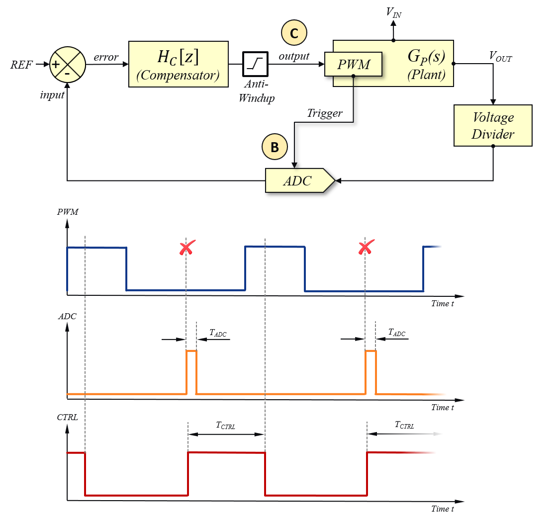
The single voltage loop controller is triggered by the PWM counter at the same time as the ADC is triggered. The control loop is executing the overhead code of calculating the first part of the compensation filter term (= A-Term) until the most recent ADC sample is available to be processed in the later part of the compensation filter term computation (= B-Term). This approach helps to shorten the overall response time of the controller measured between ADC trigger and write back event of the most recent controller result to the duty cycle register of the PWM generator. The new controller output value will then be divided by two and added to half of the period value to place the new ADC trigger point at 50% of the off-time. If the user has specified an additional offset to compensate FET driver propagation delays, this constant time-offset is also added before the ADC trigger location is updated. The the new duty cycle value will be updated immediately when the new value of the ADC trigger location is written to the PWM generator logic. By placing the ADC trigger point at 50% of the off time, the total control response is less than half a switching period, resulting in minimized phase erosion.
[back]
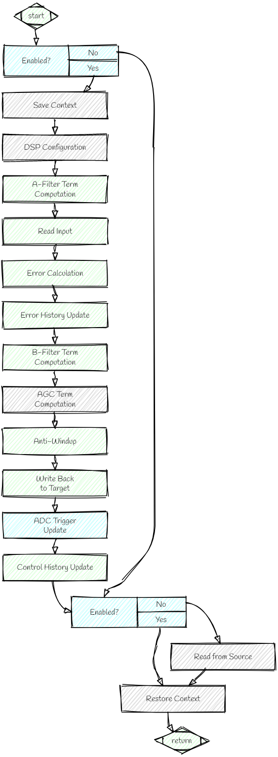
Figure 3 shows a typical flow chart of a discrete software feedback loop called at the desired control frequency. It covers the loop path from ADC trigger to PWM output shown in the block diagram above (see Figure 2) while supporting additional features like an Enable/Disable Bypass Switch or advanced features like Adaptive Gain Control (AGC).
[back]
Figure 4 shows a typical implementation of the power converter state machine and the high-speed control loop in a task scheduler based firmware environment.
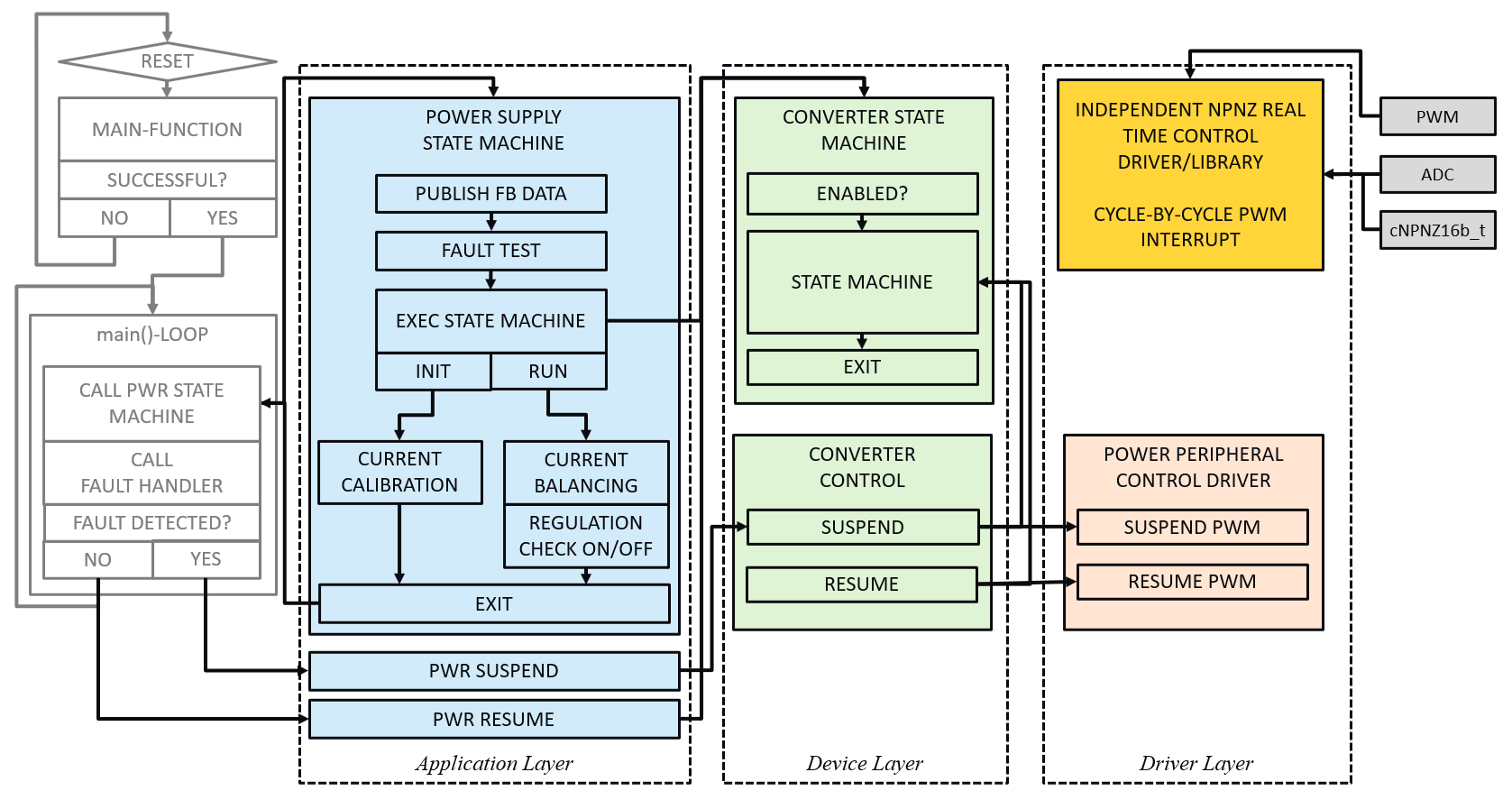
More detailed information on the library implementation, such as task and library APIs, can be found in the chapter Software Overview on the left side of this window.
[back]
(c) 2021, Microchip Technology Inc.