 |
Digital Power Starter Kit 3 Firmware
dsPIC33C Buck Converter Average Current Mode Control Example
|


|
|
Digital Power Starter Kit 3 Firmware
dsPIC33C Buck Converter Average Current Mode Control Example
|
|

This firmware demonstrates the implementation of a typical dual-loop average current mode controller used to regulate the constant output voltage of the on-board step-down converter of the Digital Power Starter Kit 3 (DPSK3). The implementation of the Current Mode Feedback Loop requires two Analog-to-Digital Converter (ADC) inputs oversampling the output voltage and inductor current of the converter and two PWM outputs (PWM high and PWM low) to drive the power converter half-bridge switch-node in synchronous mode.
[back]
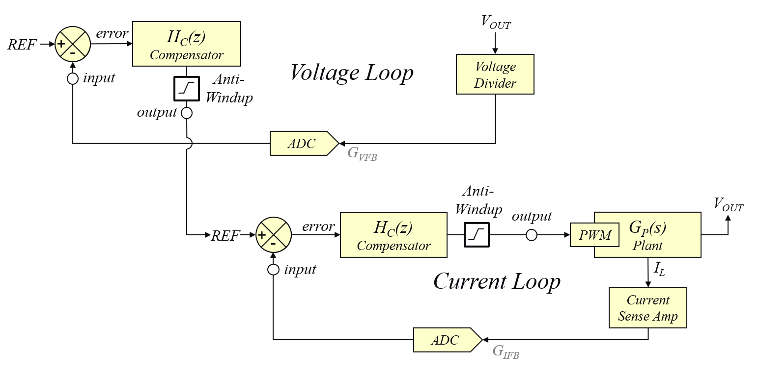
Figure 1 shows the block diagram of the buck converter average current mode controller, comprised of an outer voltage loop providing the control reference to an inner current loop. The first ADC input is used to sample the most recent level of the output voltage feedback signal. Once converted, the value is then compared against the internal voltage reference value and the inverse of the deviation between reference and feedback (= error) is pushed through the first discrete compensation filter stage. An Anti-Windup Limiter is used to limit the control loop output range to user-specified minimum and maximum limits.
The output of the outer voltage loop is passed on to the current reference input of the inner loop, where it gets compared against the most recent current feedback input read through the second ADC input. The inverse of the deviation between reference and feedback (= error) is pushed through the second discrete compensation filter stage. The output of the inner current loop is also passed through an Anti-Windup limiter, limiting the current loop control output to a user-specified range. The limiter output value is then written directly to the PWM duty cycle register of the PWM logic.
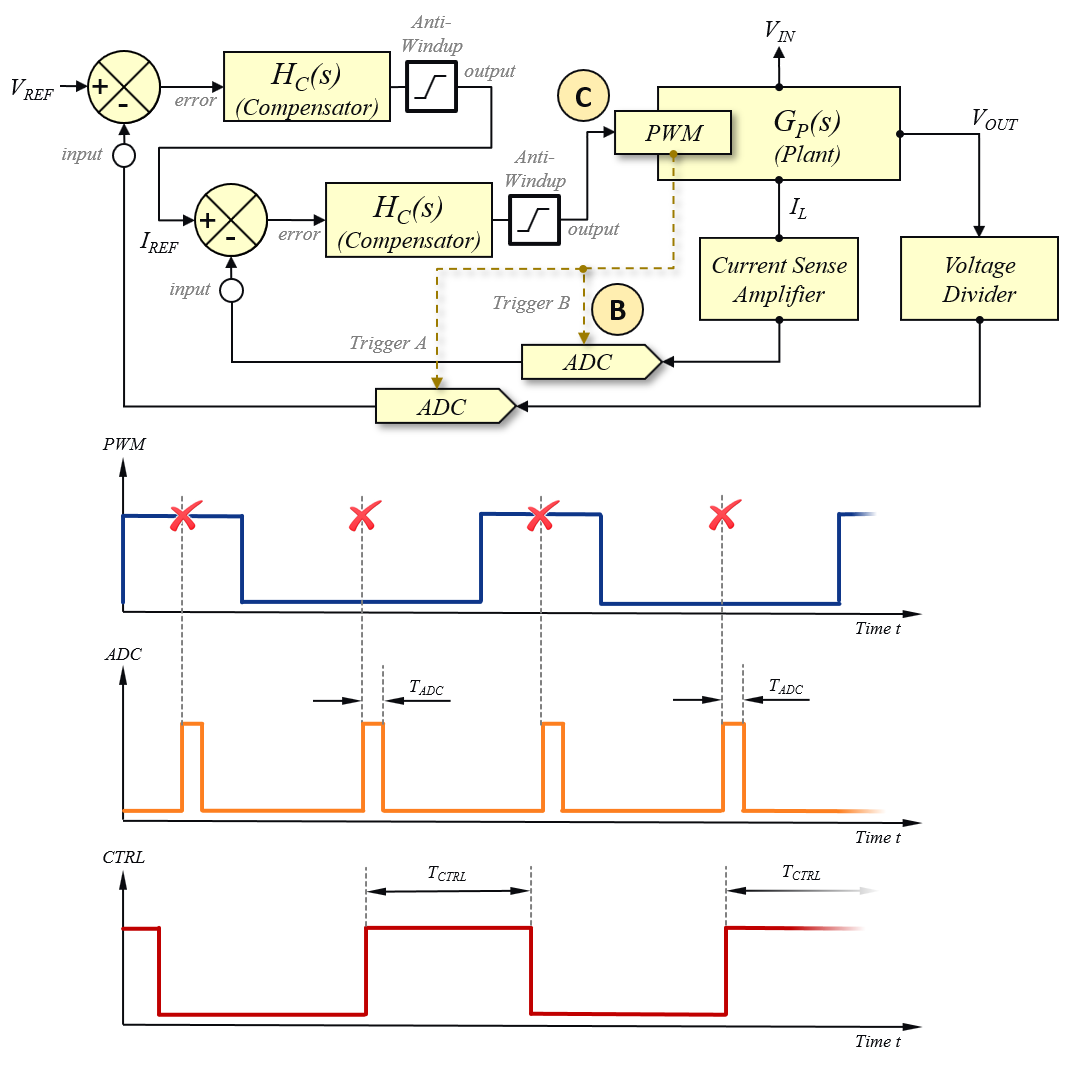
The average current mode control loop block is triggered by the PWM counter at 50% of the off-time. At this point the outer voltage loop controller is called in parallel with the output voltage ADC trigger. The first stage of the control loop is executing the overhead code of calculating the first part of the compensation filter term (= A-Term) until the most recent ADC sample is available to be processed in the later part of the compensation filter term computation (= B-Term). This approach helps to shorten the overall response time of the controller measured between ADC trigger and write back event of the most recent controller result to the duty cycle register of the PWM generator.
The output of the first stage of the control loop is then passed on to the second stage, the inner current loop. This part of the loop compares the new reference with the most recent inductor current feedback value, which was acquired previously at 50% on-time. The reciprocal of the deviation is passed through the second discrete time domain filter HC(z) and Anti-Windup Limiter. The new controller output value will then be divided by two. This value will be used to set the ADC trigger of the current loop at 50% of the on-time and added to half of the period value to place the new ADC trigger point at 50% of the off-time for the voltage loop. If the user has specified additional offsets to compensate FET driver propagation delays, this constant time-offset is added before the ADC trigger locations are updated.
The new output of the current loop will be written to the PWM duty cycle register and will be updated immediately when the new value of the ADC trigger location of the voltage loop is written to the PWM generator logic.
[back]
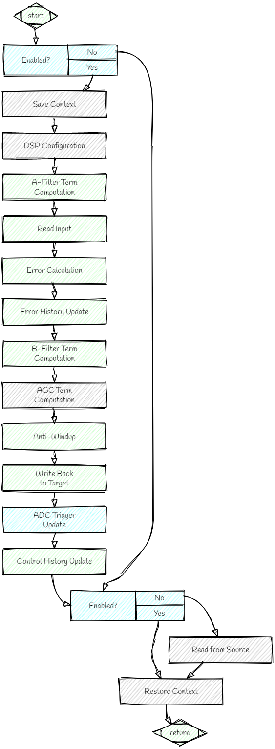
Figure 4 shows a typical flow chart of a discrete software feedback loop called at the desired control frequency. It covers the loop path from ADC trigger to PWM output shown in the block diagram above (see Figure 2 and 3) while supporting additional features like an Enable/Disable Bypass Switch or advanced features like Adaptive Gain Control (AGC).
[back]
Figure 5 shows a typical implementation of the power converter state machine and the high-speed control loop in a task scheduler based firmware environment (order right to left of Figure 5).
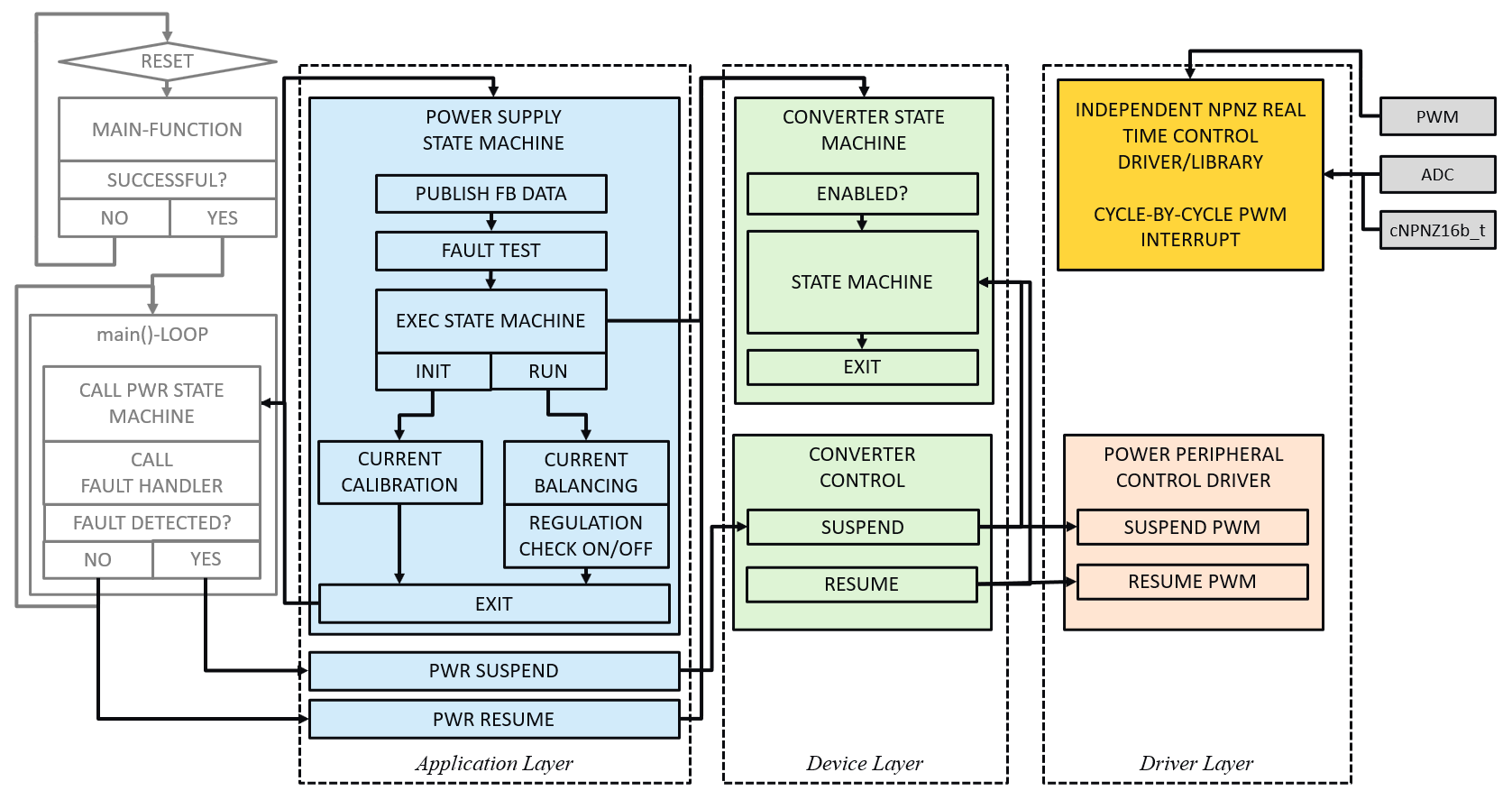
More detailed information on the library implementation, such as task and library APIs, can be found in the chapter Software Overview on the left side of this window.
[back]
(c) 2021, Microchip Technology Inc.