 |
Digital Power Starter Kit 3 Firmware
dsPIC33C Buck Converter Average Current Mode Control Example
|


|
|
Digital Power Starter Kit 3 Firmware
dsPIC33C Buck Converter Average Current Mode Control Example
|
|

This introduction covers common aspects of the firmware architecture and provides guidance on specific firmware module documentation included in this document.
Establishing a digital control system for a switched-mode power supply using a programmable microcontroller requires some specific considerations. Foremost, it is vital to allow the switching signal generation and high-speed real-time control loop to run freely and uninterrupted while background activity of additional, less time critical functions such as communication and housekeeping also gets enough bandwidth to be executed within their required timing tolerances.
This is achieved by splitting up processes among different functional sections of the device such as independent peripheral modules, the CPU itself and the multi-priority level interrupt controller of the dsPIC33® Digital Signal Controller. Peripherals are function blocks such as the PWM generator logic, Analog-to-Digital Converters (ADC), Digital-to-Analog Converters (DAC) or communication interfaces such as Universal Asynchronous Receiver-Transmitter (UART), Inter-Integrated Circuit (I2C), Serial Peripheral Interface (SPI) or Controller Area Network (CAN), which all support some degree of independent operation from the CPU but may all depend on the same system clock. A second class of peripherals are truly independent such as operational amplifiers, analog comparators or glue logic cells, which can operate even if the CPU and system clock are turned off.
This arrangement of different function blocks with different degrees of independence allows the generation of highly deterministic, high resolution switching signals commutating the power supply switch node while running multiple other processes in parallel without having one influencing the other.
[back]
The critical component is where CPU activity needs to get shared between different software-driven processes such as housekeeping background tasks, processing communication protocols and the software-based real-time feedback loop. As the CPU can only execute one instruction at the time, this process alignment is managed by the multi-priority level interrupt controller mentioned above.
Depending on the device generation, the CPU architecture of dsPIC33® provides between 8 and 16 priority levels on which code can be executed. Interrupt nesting allows higher priority processes to interrupt lower priority processes. While a higher priority process is executed, the lower priority process is stopped at the point when the interrupt occurred. Its execution continues seamlessly after the high priority process has been completed.
Priority level #0 is the lowest one and is continuously occupied by the main program, which is automatically started when the device comes out of reset. The highest priority level (#8 or #16) is reserved for so-called uninterruptible processes, such as fatal errors caused by a divide by zero, an address error, stack error or oscillator failure, which are the equivalent to a PC's blue screen error. These fatal errors will all lead to a CPU reset if not handled in software. All remaining priority levels can be selected by the user and used to arrange software processes to account for their individual importance, timing tolerance or required response time.
Depending on how many priority levels are staggered for simultaneous execution, the respective execution time of a process will be more deterministic the higher its priority level, resp. less deterministic the lower its priority level is.
[back]
The CPU is running executing the main loop of the program on priority level #0. This routine is interrupted by another process called on priority level #2. Hence, the level #0 process is suspended until the process on priority level #2 has been executed and the CPU returns to priority level #0.
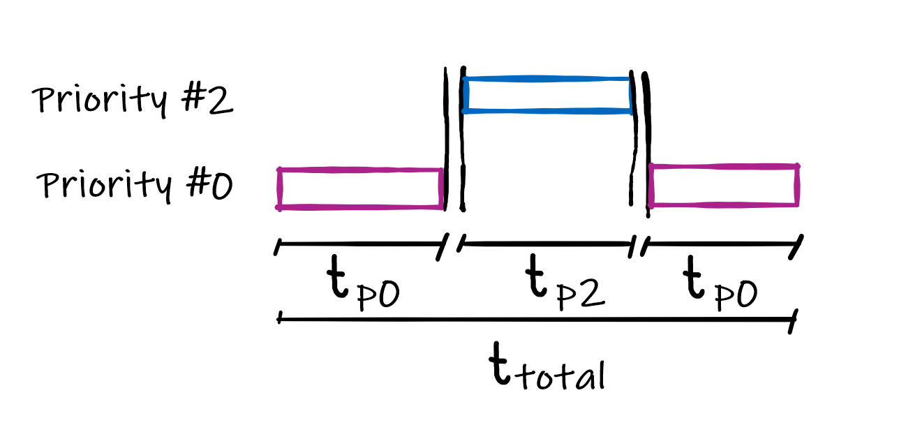
While the total execution time of the process on priority level #2 t(p2) in this example is deterministic, as it will be executed uninterrupted, the total execution time of the process on priority level #0 t(p0) will now be the sum of both processes t(p0) + t(p2). Hence, the priority level #2 process will behave more deterministic than the priority level #0 task.
[back]
However, if a even higher priority level #6 process is called while the process on priority level #2 is still active, the priority level #2 process gets also interrupted and suspended until the execution of the priority level #6 process has been completed.
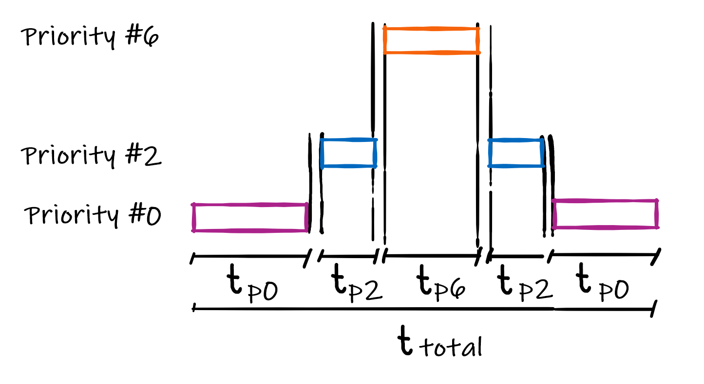
Now the execution time of priority level #6 process is deterministic while the execution time of the priority level #2 process includes the execution time spend to execute the priority level #6 process. The total execution time of the priority level #0 process is now the sum of t(p0), t(p2) and t(p6).
[back]
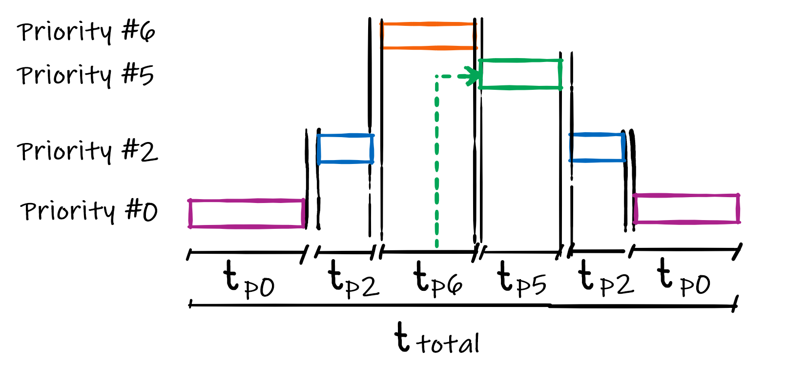
To make things even more complex, we now introduce a fourth, simultaneous process on interrupt level #5, which occurs while the higher interrupt priority level #6 is still active. As priority #6 is higher than level #5, the priority level #5 process will be pending until the higher priority level #6 process has been completed. However, instead of stepping back down to the suspended priority level #2 process, the newly occurred priority level #5 process is executed first before the priority level #2 process is continued. The main program will be resumed once all higher priority levels have been completed.
[back]
As stated above, in a switched-mode power supply the real-time control loop always requires to have the highest priority in the system to ensure stable operation of the digital compensation filter including all potentially necessary real-time responses applied to the switching operation. In multi-loop control systems such as average current mode, multiple high-priority processes are usually triggered by the switching signal generator (i.e. PWM module) being distributed across a switching cycle to ensure uninterrupted, collision-free execution of each feedback loop.
The next lower level is commonly reserved for tasks, which are less time critical than the real-time control loops but only allow a limited amount of execution time jitter and require to be executed at a known, deterministic frequency. This is commonly true for the power supply state machine and fault monitor. This class of processes are called high-priority tasks.
The lowest levels are reserved for uncritical tasks or tasks not relying on deterministic execution such as communication protocol responses, self-diagnostic functions, human-machine interface (HMI) operations or housekeeping functions.
Each of these three basic levels may accept a certain amount of jitter in its execution period and or execution repetition frequency. Both properties may influence the reliability of a process and needs to be examined carefully to ensure the complete firmware remains stable, reliable and responsive. Slower tasks with comparatively long execution periods usually accept larger execution period jitter as well as are less reliant on a precise execution repetition frequency and therefore can be placed at lower priority levels. the more time critical a process, the shorter it execution time usually is, allowing to place it at higher priorities, frequently interrupting the lower priority tasks.
For example, processing a communication response includes multiple different steps such as receiving a certain number of data bytes, performing a cyclic redundancy check (CRC) validating, parsing command and data content, generating the response, handing the response back to the communication interface, monitoring the transmission of the response. Depending on the type of interface and transmission mechanism used, this process can take many milliseconds to complete and may occur every couple of seconds. Im comparison, a real-time control loop of a power supply may only take a couple of 100 nanoseconds to be executed at a repetition frequency of several 100 kHz. Hence, processing the communication protocol will potentially get interrupted thousands of times in one communication cycle.
Hence, aligning low and high priority processes requires to break up the longer, more tolerant tasks in smaller sub-processes, which can be called in defined sequences, the so-called states. These states are then managed and monitored by individual sequencers called state machines. The more processes need to run in parallel, the smaller the individual states of a state machine need to be to allow most effective interleaving of parallel processes.
[back]
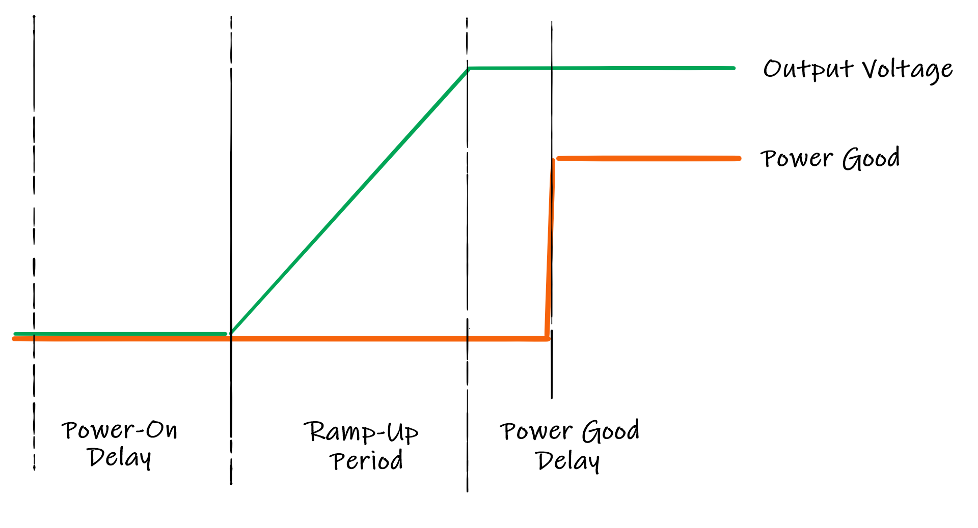
The state machine managing the power converter of the development board is implemented as high priority task in the task execution scheme described above. This state machine is tuned for constant voltage regulation. Hence, it offers user-programmable soft-start support including power on-delay, ramp up slope and power good delay, which allows users to tune the startup behavior and include this module in a larger sequencing scheme. The state machine further supports hardware triggered events such as an external ENABLE pin and a POWER GOOD output. Both active pins can be configured in push-pull (default) or open drain mode.
The startup configuration can be configured as shown in the following drawing:
[back]
During execution, it goes through the following steps in chronological order:
In this step the control loop parameters are reset to their defaults, PWM outputs are turned off but the PWM is still running, continuously triggering the ADC to keep sampling input and output voltage as well as board temperature.
[back]
This is the 'fall-back' state from which the buck converter will be restarted once it has been started successfully and has been shut down due to a fault condition (e.g. input under/over voltage or over temperature condition)
[back]
After Reset, the state machine waits for all fault flags to be cleared and the enable and GO bits to be set. If the AutoRun option of the power converter data object is enabled, the GO bit will be set automatically as soon as the Enable bit is set.
[back]
Once the power converter fault flags have been cleared the state machine will execute the startup procedure starting with the Power On Delay. This is a simple, counter-based delay during which the converter will remain inactive but the fault handler will observe the values generated by the ADC for occurring fault conditions. If a fault condition is detected, the state machine will be reset to state Reset and all fault flags have to be cleared first before the state machine is allowed to proceed with the start-up procedure.
[back]
After the Power-On delay has expired, input and output voltage will be measured. If some residual output voltage is detected, an ideal duty cycle is calculated which will produce an output voltage matching the measured value. The power controller will be 'pre-charged' with the result of this calculation by programming the estimated duty cycle into the control history and set the initial PWM duty cycle output. When the power supply is then turned on, it will tune into the residual output voltage and smoothly ramp up the output voltage from its most recent level without causing reverse current spikes or glitches in output voltage levels.
[back]
Now the digital feedback loop and PWM are enabled and the closed loop system reference value is incremented with every execution of the state machine (typical interval = 100 µsec). The control loop has been adjusted to operate with a cross-over frequency of >10 kHz matching the maximum perturbation frequency allowed to keep the control system stable.
The control loop is active during the entire ramp-up phase. A controlled soft-start will therefore also compensate potential load changes which might occur when the output voltage passes the minimum operating voltage of the load.
When the control loop is enabled, the fault handler will continuously compare the most recent output voltage against the given feedback loop reference. Should the deviation between both exceed a give limit for a given amount of time, a Regulation Error will be tripped and the power supply will shut down, assuming a system failure such as a shorted output, a permanent over load condition or insufficient power supply input has occurred. The shut-down of the power supply will also reset the state machine to Reset state, from which all fault flags have to be cleared first, before the state machine is allowed to initiate a new start-up attempt. Each repeated start-up event will go through all state described above, including the Power-On Delay.
[back]
This additional state is only executed in average current mode control (ACMC), where the power supply could potentially run into current limit conditions while ramping up the output voltage. It is also covering the output current soft start for constant current applications such as battery chargers or LED and laser drivers.
The mechanism of the state machine will seamlessly switch from voltage ramp up to current ramp up when the control system hits the current limit during the voltage ramp up. In this state the state machine will ramp up until it matches the declared maximum output current, at which point the state machine will more on to the Power Good Delay (PGD) state.
Use Case Example Battery Charger:
In a typical battery charger application the maximum output voltage will be defined by the maximum charing voltage and total voltage level of the battery stack topology. The Anti-Windup limits are set for limiting the current loop references where the starting value is set to the minimum charging current value equivalent. When the power supply ramps up, this current limit will be hit and the state machine will switch to this current ramp up state.
The user can define a maximum current limit for this ramp up, which, in most cases, will be set by some battery management firmware driver. The ramp up slew rate of the current is defined in the same way as the voltage ramp up slew rate in the hardware abstraction layer. When the declared limit has been reached, the power supply state machine will pass through the Power Good Delay (PGD) period entering the Online state.
In the Online state external firmware (e.g. battery management firmware) will have full control over the current reference able to apply the charing profile. In pulsed charging mode, the power supply device driver API provides the two functions SUSPEND and RESUME to turn the charger on and off at low frequency, where the duty ratio of the pulse charging must be adjusted by the external firmware module.
The transition between constant current and constant voltage charging will automatically occur when the declared voltage reference matches the most recent output voltage at which point the current loop is not operating in current limit mode anymore. In this condition the power supply will behave like a normal average current mode controlled converter. With increasing charge, the output current will steadily drop until passing the cut-off threshold level. This threshold level must be managed by the external firmware module.
The continuous closed loop average current mode control structure also allows to power loads while charging as the feedback loop can seamlessly transition between constant current and constant voltage mode.
[back]
After the reference voltage has been increased to the pre-defined nominal level, the state machine switches over into the Power Good Delay period. This is another, simple, counter-based delay where the control loop is kept in steady state waiting for the delay period to expire.
During the Power Good period no significant variation of the output voltage is allowed. Any glitch exceeding the allowed maximum deviation will reset the Power Good timer. Multiple Power Good timer resets are considered to indicate a system failure, which forces a power supply restart. During this period the fault handler also monitors all other fault objects such as regulation deviation, input over- and under voltage, output over current and over temperature conditions.
When the Power Good timer expires and no error has been detected, the Power Good GPIO will be set HIGH and the state machine enters the Online state.
[back]
After the Power Good Delay has expired, the converter drops into nominal operation. In this condition it continuously observes the reference value for changes. Should any other part of the firmware change the controller reference, the state machine will softly tune into the new level instead of hard-switching the reference by incrementing/decrementing the control reference until the value meets the new commanded reference value.
[back]
If the power controller is shut down and reset by external commands (e.g. fault handler detecting a fault condition or through user-interaction), the state machine is switching into the SUSPEND state, which disables the PWM outputs and control loop execution, clears the control histories and resets the state machine back to Reset
[back]
The Digital Power Starter Kit 3 is equipped with a set of independent protection circuits preventing hardware damages in case of floored peripheral configurations or unstable control loops, to give users the safety of experimenting without risk or damaging the hardware.
Most of these protection circuits are located on the bottom side of the board and are managed by an additional PIC24 microcontroller. This housekeeping MCU needs to startup first and clear the protection circuit before the dsPIC section of the board is enabled. The following figure shows the real start-up timing of the DSPK3 hardware. When input power is applied to the board, there is a ~500 ms long pause, during which the auxiliary power supplies are ramping up, the PIC24 housekeeping device wakes up, analyzes the system conditions, clears the protection logic and finally allows the dsPIC to run.
After the Firmware Start event, the dsPIC firmware starts up and initializes peripherals and software modules. After this short delay, the Soft-Start timing pattern is rolled out by the power converter state machine as described above.
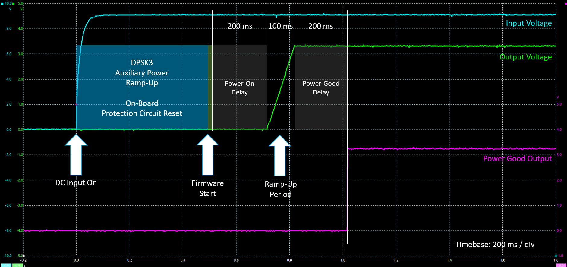
Signals measured at:
[back]
The fault handler is an independent firmware task, based on a fault monitor library, which is used to define certain so-called Fault Objects. A 'Fault Object' represents a value of a special function register or global user variable, which will monitored and validated by the Fault Monitor Library. The Library supports different comparisons for validation, such as
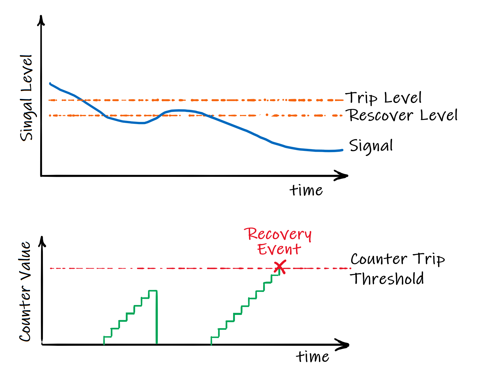
Fault Monitor source values are either compared against a user-defined constant (static threshold), or another variable (dynamic threshold). THe Fault Monitor further supports two thresholds, one defining the Fault Trip Level and a second Fault Recovery Level. Depending on the type of comparison selected, the range between both thresholds is either interpreted as hysteresis or range. (see Fault Handler Library for details)
The fundamental mechanism of detecting fault conditions and creating trip and recovery responses is based on a simple, adjustable detection filter, which does not influence the monitored value but delays the response of the software. Depending on the type of value monitored, the firmware may need to react sooner or later while the fault detection sensitivity needs to be adjusted accordingly to prevent the power supply from unintended shut downs.
The delay filter counts successive threshold violations, comparing the most recent counter value against an absolute, user-defined maximum. When one sample of the monitored value does not violate the given threshold, the counter is reset and starts incrementing from zero at the next threshold detection. When the monitored value remains violating the given threshold until the counter reaches or exceeds the defined maximum counter value, the power supply shut down event is triggered, turning off PWM outputs and control loops and resetting the state machine, waiting for the fault condition to disappear.
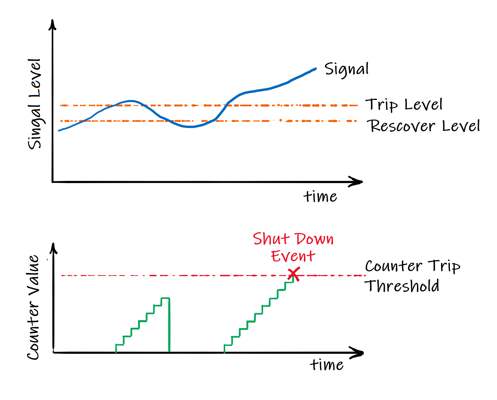
Recovering from a fault condition uses the same mechanism, but provides its individual set of parameters. Thus, fault trip responses can be adjusted to be aggressive while recovery events can be further delayed to prevent the end-product from falling into an undesired, high frequency shut-down/restart cycle.
[back]
This firmware utilizes a so-called hardware abstraction layer, allowing users to quickly change fundamental system parameters, adopt pin-out and hardware changes and even migrating the firmware across different designs without having to modify the actual source code.
Any change to the firmware and fundamental operation of the reference design or development board, including reprogramming of the nominal output voltage can be done by editing the hardware-specific values in the hardware description header file **'[Board-ID]_hwdescr.h'** located in **'Project Manager => Header Files/Config'**
Converter settings in this file are defined as physical values such as Volt, Ampere, Ohm, etc. Each defined value is converted into binary numbers by so-called macros, at compile time. Thus, users do not have to convert values manually.
A detailed description of all available settings, their valid range and purpose can be found in chapter Hardware Abstraction Layer in this documentation.
To program the converter to provide a nominal output voltage different from the default setting, follow these steps:
The setting for the nominal output voltage is found in lines #484 through #486.
#define BUCK_VOUT_NOMINAL           (float)3.300   // Nominal output voltage
#define BUCK_VOUT_TOLERANCE_MAX     (float)0.500   // Output voltage tolerance [+/-]
#define BUCK_VOUT_TOLERANCE_MIN     (float)0.100   // Output voltage tolerance [+/-]
The tolerance settings above include the transient response at a maximum load step. The value for maximum output voltage tolerance (e.g. 'BUCK_VOUT_TOLERANCE_MAX') is monitored by the fault handler. Should the output voltage reading divert from the most recent reference voltage value by more than the given range, the converter will be shut down and a REGULATION ERROR will be indicated. The power supply will automatically recover as soon as the fault condition has been cleared and the recover delay period specified by BUCK_REGERR_RECOVERY_DELAY in the hardware description header file has expired.
(line numbers given may be subject to change)
[back]
The control loop source code is configured and generated by the PowerSmart™ - Digital Control Library Designer (PS-DCLD) software.
This additional design software is available for download on Github Pages:
Once installed, the controller configuration can be modified. The most recent configuration can be opened from within the MPLAB® X IDE by right-clicking on the file (e.g. **'v_loop.dcld'**) located in the Important Files folder of the MPLAB® X Project Manager. When right-clicked, select Open In System to open the configuration in PowerSmart™ DCLD.
Please refer to the user guide of PowerSmart™ DCLD which is included in the software and can be opened from the help menu of the application.
[back]
This code examples includes an alternative, proportional control loop which is commonly used during measurements of the frequency response of the power plant. When the following define is set to true, the common main control loop is replaced by the proportional controller. The code has to be rebuilt and programmed to run the measurement.
[Board-ID]_hwdescr.h: #define PLANT_MEASUREMENT false
PLEASE NOTE:
PROPORTIONAL CONTROLLERS ARE BY DEFAULT UNSTABLE AND NOT SUITED TO REGULATE THE OUTPUT OF A POWER SUPPLY UNDER NORMAL OPERATING CONDITIONS. DURING A PLANT MEASUREMENT IT IS MANDATORY THAT INPUT VOLTAGE AND LOAD REMAIN STABLE AND DO NOT CHANGE.
FOR MORE INFORMATION ABOUT HOW TO CONDUCT A POWER PLANT MEASUREMENT, PLEASE READ THE SECTIONS IN THE PowerSmart™ DCLD USER GUIDE.
[back]
(c) 2021, Microchip Technology Inc.